

Touch display device
A technology of a touch display device and a touch layer, which is applied in the fields of instruments, electrical digital data processing, and data processing input/output processes, etc., can solve problems such as poor touch operation experience, and achieve the effect of improving the touch point reporting rate.
- Summary
- Abstract
- Description
- Claims
- Application Information
AI Technical Summary
Problems solved by technology
Method used
Image

Examples
no. 1 example
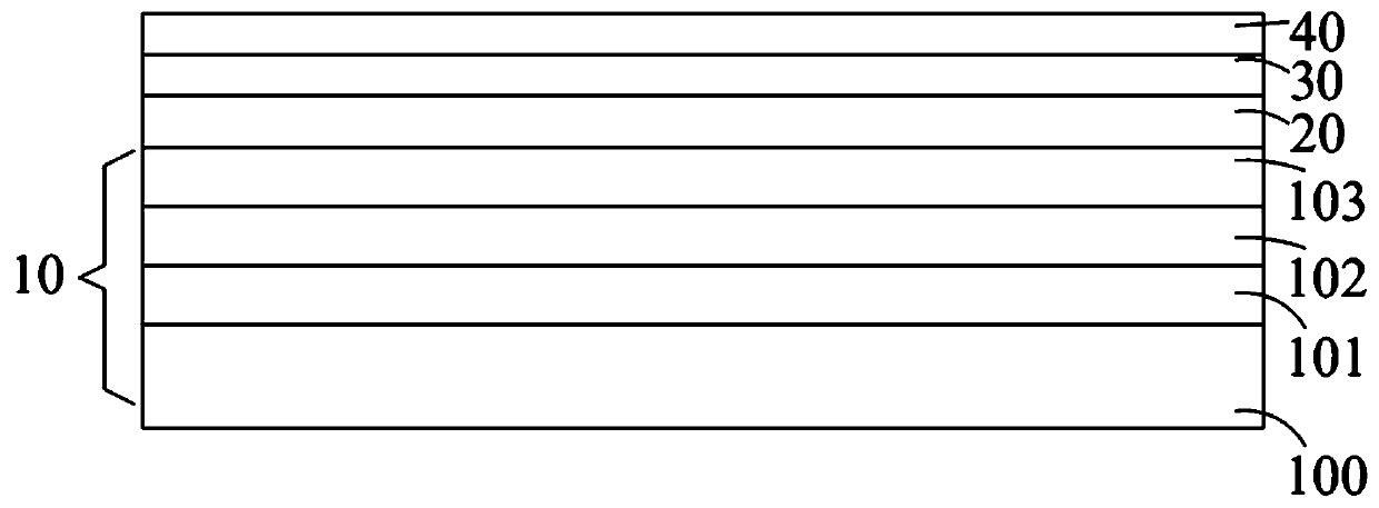
[0084] see figure 1 , which is a schematic diagram of the touch display device of the present application. The touch display device includes an OLED display panel 10 , a touch layer 20 , a polarizer 30 and a protective cover 40 .
[0085] The OLED display panel 10 includes a substrate 100 , a TFT array layer 101 , an OLED array layer 102 and an encapsulation layer 103 .
[0086] The substrate 100 is a flexible substrate. The thin film transistor array layer 101 is disposed on the substrate 100, and the thin film transistor array layer 101 includes a plurality of thin film transistors arranged in an array. The OLED array layer 102 is disposed on a side of the TFT array layer 101 away from the substrate 100 . The organic light emitting diode array layer 102 includes a plurality of organic light emitting diodes arranged in an array, and the plurality of organic light emitting diodes includes a plurality of independent anodes, an organic light emitting layer disposed on each an...
no. 2 example
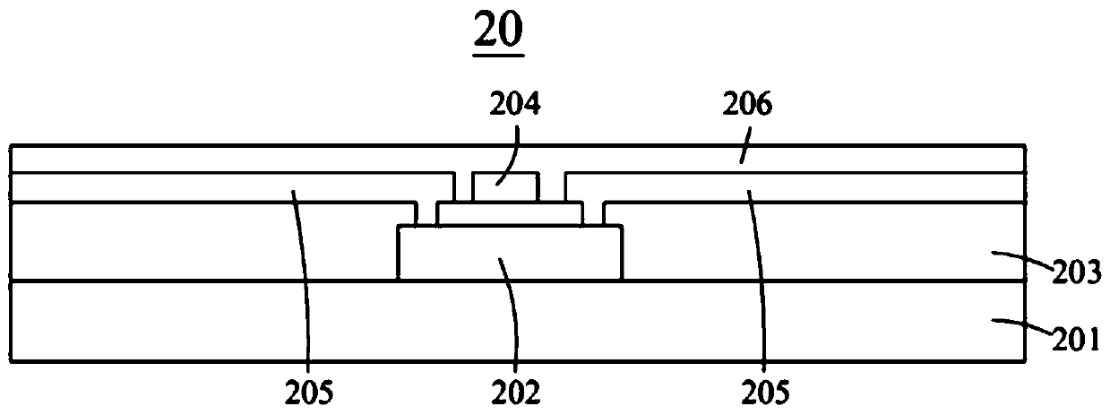
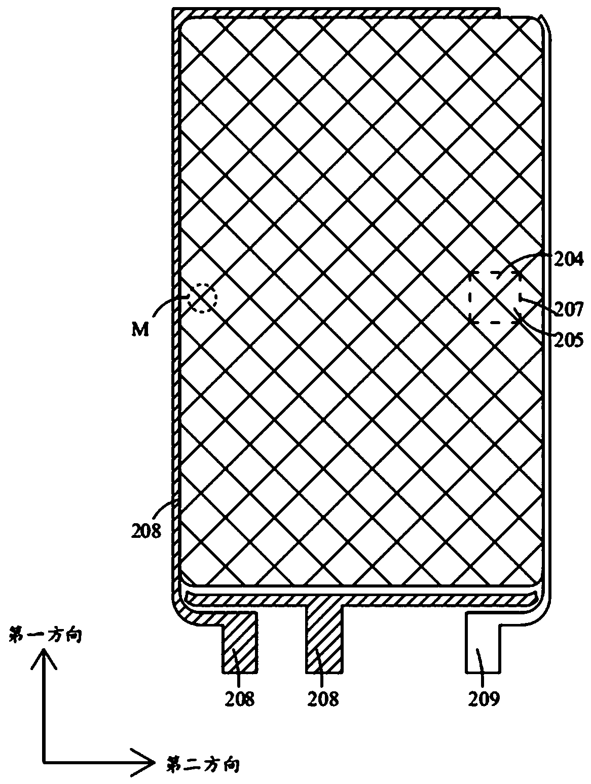
[0090] see image 3 , which is figure 1 A schematic diagram of the first structure of the touch layer of the touch display device shown. The first electrodes 204 of the plurality of touch units 207 arranged in the same row in the first direction are electrically connected to form a first electrode channel, and the second electrodes of the plurality of touch units 207 arranged in the same row in the second direction 205 are electrically connected to form a second electrode channel. Both ends of each first electrode channel are connected to the first lead 208 , and one end of each second electrode channel is connected to the second lead 209 , that is, the touch layer adopts a 2T1R structure.
[0091] In this embodiment, the first electrodes are driving electrodes, and the second electrodes are sensing electrodes. There are 17 first electrode channels in the second direction, and 37 second electrode channels in the first direction, wherein the 1st second electrode channel to t...
no. 3 example
[0095] see Figure 4 , which is figure 1 A schematic diagram of the second structure of the touch layer of the touch display device shown. Figure 4 Touch layer shown with image 3 The touch layers shown are basically similar, Figure 4 and image 3 The structure of the touch layer shown is different in that one end of each first electrode channel is connected to the first lead 208 , and one end of each second electrode channel is connected to the second lead 209 , that is, the touch layer adopts a 1T1R structure. The layout design of the first electrode and the second electrode in this embodiment is consistent with image 3 The shown touch layer is the same, and the way of group scanning is also the same as that of the second embodiment.
[0096] In this embodiment, the node mutual capacitance M that takes the longest time to charge to 95% of the input voltage on the touch layer is located at a position far from the input signal of the touch chip, for example, at the fir...
PUM
| Property | Measurement | Unit |
|---|---|---|
| Resistance | aaaaa | aaaaa |
| Resistance | aaaaa | aaaaa |
| Resistance | aaaaa | aaaaa |
Abstract
Description
Claims
Application Information