SRAF image generation method and system and electronic device thereof

An image generation and layout technology, which is applied in 2D image generation, image data processing, electrical digital data processing, etc., can solve the problem that SRAF images cannot maintain layout symmetry, etc., to ensure accuracy and symmetry, and maintain symmetry. , Flexibility for a wide range of effects

Active Publication Date: 2020-09-01
SHENZHEN JINGYUAN INFORMATION TECH CO LTD
View PDF3 Cites 1 Cited by
  • Summary
  • Abstract
  • Description
  • Claims
  • Application Information

AI Technical Summary

Problems solved by technology

[0005] In order to solve the technical problem that the SRAF image generated by the existing method cannot maintain the orig

Method used


Image

  • SRAF image generation method and system and electronic device thereof
  • SRAF image generation method and system and electronic device thereof
  • SRAF image generation method and system and electronic device thereof

Examples


Embodiment Construction

[0043] In order to make the object, technical solution and advantages of the present invention clearer, the invention will be further described in detail below in conjunction with the accompanying drawings and implementation examples. It should be understood that the specific embodiments described here are only used to explain the present invention, not to limit the present invention.

[0044] The invention provides a method for generating SRAF images, which is suitable for solving the problem of generating SRAF images with symmetrical layouts in the photolithography field of semiconductor manufacturing.

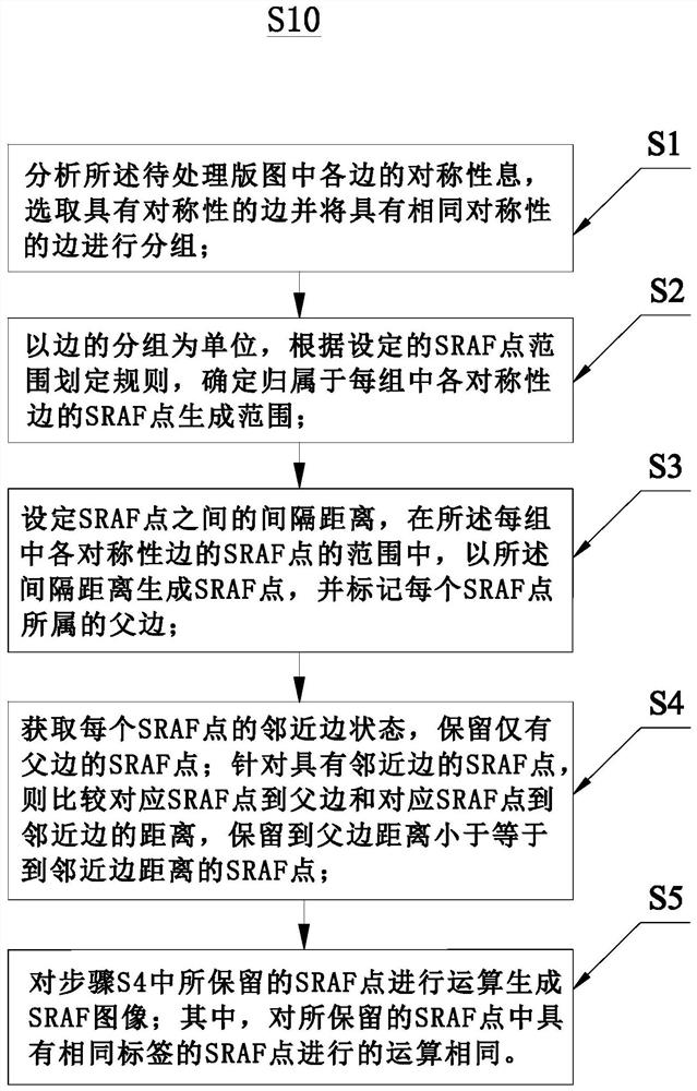
[0045] see figure 1 , a SRAF image generation method S10 of the present invention is described with the provided layout to be processed, and specifically includes the following steps:

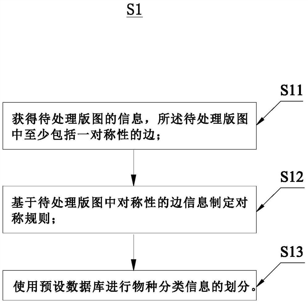
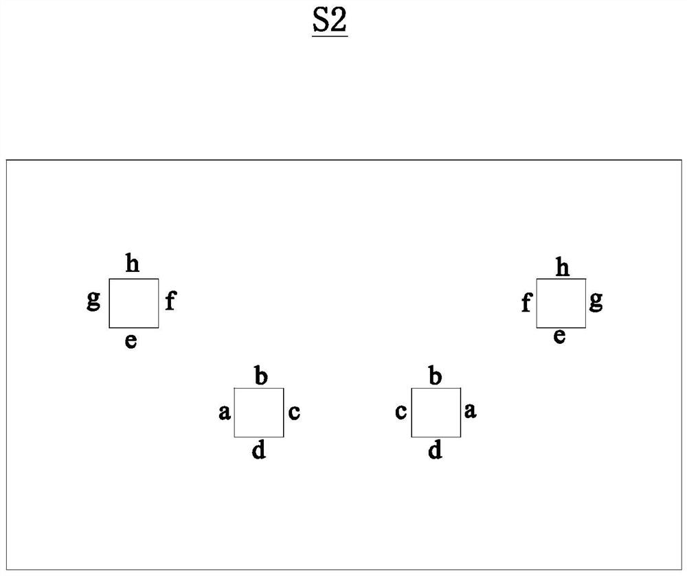
[0046] Step S1: Analyzing the symmetry of each edge in the layout to be processed, selecting edges with symmetry and grouping the edges with the same symmetry; wherein, the edges in the layo...


PUM


Abstract

The invention relates to the field of photoetching of semiconductor manufacturing, in particular to an SRAF image generation method and system and an electronic device thereof. The SRAF image generation method comprises the following steps: analyzing symmetry information of each edge in a to-be-processed layout, and grouping based on the edges with symmetry; determining an SRAF point generation range belonging to each group of edges according to a preset SRAF point range delimiting rule; setting a spacing distance between the SRAF points, generating the SRAF points according to the spacing distance, and marking a father edge to which the SRAF points belong and labels corresponding to the SRAF points; reserving an SRAF point with only a father edge; for the SRAF points with the adjacent edges, comparing the distances from the corresponding SRAF points to the father edge and the adjacent edges, and reserving the SRAF points with the distances from the father edge to the adjacent edges smaller than or equal to the distances from the corresponding SRAF points to the adjacent edges; and generating an SRAF image in combination with the SRAF point and an SRAF image generation algorithm. According to the SRAF image generation method and system and the electronic device thereof, the problem that the layout symmetry of the SRAF image generated by the existing method cannot be maintainedcan be effectively solved.

Description

【Technical field】 [0001] The invention relates to the photolithography field of semiconductor manufacturing, in particular to a method, system and electronic device for generating an SRAF image. 【Background technique】 [0002] The photolithography process is the most important process in the existing large-scale integrated circuit manufacturing process, that is, an important means to transfer the design pattern of the integrated circuit on the mask to the silicon wafer through the photolithography machine. When the integrated circuit design pattern on the mask is imaged on the silicon wafer through the projection objective lens of the lithography machine, due to the small feature size of the pattern on the mask, the light diffraction phenomenon is significant. When some high-order diffracted light cannot participate in imaging due to the aperture limitation of the projection objective optical system, the imaging on the silicon wafer will produce distortion and indistinguisha...

Claims


Application Information

Patent Timeline
IPC IPC(8): G06T11/00G06F30/392
CPCG06T11/00
Inventor 黄晔丁明
Owner SHENZHEN JINGYUAN INFORMATION TECH CO LTD
Why Eureka
Try Eureka