A kind of 3D NAND memory and manufacturing method thereof

A 3DNAND and manufacturing method technology, applied in semiconductor devices, electrical solid-state devices, electrical components, etc., can solve the uniformity and continuity defects of epitaxial structures, increase the difficulty of etching stack structure, and difficult to control the thickness of the back selective gate oxide, etc. problem, to achieve the effect of improving uniformity and improving life.

Active Publication Date: 2021-05-07
YANGTZE MEMORY TECH CO LTD
View PDF4 Cites 0 Cited by
  • Summary
  • Abstract
  • Description
  • Claims
  • Application Information

AI Technical Summary

Problems solved by technology

[0003] The traditional method of realizing the communication between the channel structure and the substrate usually faces the problem of the uniformity and continuity of the epitaxial structure, or the difficulty of controlling the thickness of the back selection gate oxide.
In the multi-layer trench hole process, it will also face the problem of increased etching difficulty of the stacked structure

Method used


Image

  • A kind of 3D NAND memory and manufacturing method thereof
  • A kind of 3D NAND memory and manufacturing method thereof
  • A kind of 3D NAND memory and manufacturing method thereof

Examples


Embodiment 1

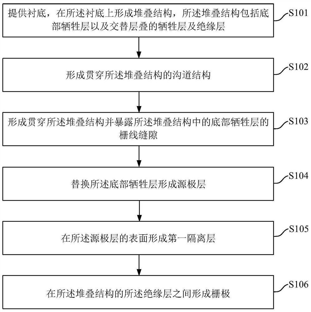
[0117] This embodiment provides a method for manufacturing a 3D NAND memory, such as figure 2 As shown, the method includes the following steps:

[0118] Step S101: providing a substrate, and forming a stacked structure on the substrate, the stacked structure including alternately stacked sacrificial layers and insulating layers;

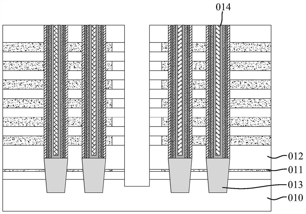
[0119] refer to image 3 Firstly, a substrate 100 is provided, and a stack structure 102 is formed on the substrate 100 . In this embodiment, the substrate 100 may be a substrate of silicon, single crystal silicon-on-insulator or other suitable materials. Moreover, a P-type well on the top of the substrate 100 and an N-type well below the P-type well (not shown in detail) may also be formed in the substrate 100 . The stacked structure 102 may have 64 layers, 96 layers, 128 layers or even more layers.

[0120] still refer to image 3When forming the stacked structure 102 above, the bottom sacrificial layer 101 is firstly formed on the substrate...

Embodiment 2

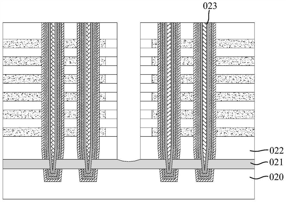
[0141] This embodiment provides a 3D NAND memory, which can also refer to Figure 3 ~ Figure 17 , the memory consists of:

[0142] a substrate; a stack structure formed above the substrate, the stack structure comprising a source layer formed on the substrate, a first isolation layer formed above the source layer, and a first isolation layer formed on the first alternately stacked gate layers and insulating layers over an isolation layer;

[0143] a channel structure running through the stack structure;

[0144] a common source, the common source runs through the stack structure and communicates with the substrate;

[0145] Wherein, the source layer includes a first portion located below the stack structure and a second portion formed in the channel structure and communicated with the channel structure, and, in the stacking direction of the stack structure, The width of the second portion is greater than the width of the first portion.

[0146] refer to Figure 3 ~ Figure...


PUM

PropertyMeasurementUnit
thicknessaaaaaaaaaa

Abstract

The present invention provides a 3D NAND memory and a manufacturing method thereof. In the method, a stacked structure comprising a bottom sacrificial layer and alternately stacked sacrificial layers and insulating layers formed above the bottom sacrificial layer is formed on a substrate, and the bottom sacrificial layer is replaced by The source layer is oxidized, and a first isolation layer is formed on the surface of the source layer to realize the function of the back selection gate oxide. The method is beneficial to control the thickness of the first isolation layer and improve the uniformity of the first isolation layer, thereby facilitating the uniform inversion of the source electrode layer and ensuring the channel of electrons in the read and write operations of the memory. The thickness and uniformity of the source layer caused by the thickness of the back selection gate oxide layer are solved, and the continuity of the P-type well and the supply of holes during the erasing process can be realized. At the same time, the source layer is formed in the channel structure along the stacking direction, which increases the contact area between the source layer and the channel layer, and enhances the electrical connection between the source layer and the channel layer.

Description

technical field [0001] The invention relates to the field of semiconductor integrated circuit manufacturing, in particular to a 3D NAND memory and a manufacturing method thereof. Background technique [0002] As the feature size of devices in integrated circuits continues to shrink, 3D memory technologies that stack multiple planes of memory cells to achieve greater storage capacity and lower cost per bit are increasingly favored. 3D memory is a technology for stacking data units. Currently, more than 32 layers, or even 72, 96, 128 or more layers of data units can be stacked. As the number of stacked layers increases, the lead-out of the memory structure that runs through the stacked structure faces increasing challenges. [0003] The traditional method of realizing the communication between the channel structure and the substrate usually faces the problem of defects in the uniformity and continuity of the epitaxial structure, or the difficulty in controlling the thickness ...

Claims


Application Information

Patent Timeline
Patent Type & Authority Patents(China)
IPC IPC(8): H01L27/1157H01L27/11582
CPCH10B43/35H10B43/27
Inventor 孙中旺夏志良王迪周文犀
Owner YANGTZE MEMORY TECH CO LTD
Why Eureka
Try Eureka