Broadband transparent wave-absorbing material based on double-layer conductive film
A wave-absorbing material and conductive film technology, applied in the direction of electrical components, antennas, etc., can solve the problems of difficult large-scale preparation, non-transparent visible light, poor wave-absorbing performance, etc., and achieve no need for etching processing, small visual impact, and easy preparation Effect
- Summary
- Abstract
- Description
- Claims
- Application Information
AI Technical Summary
Problems solved by technology
Method used
Image

Examples
Embodiment 1
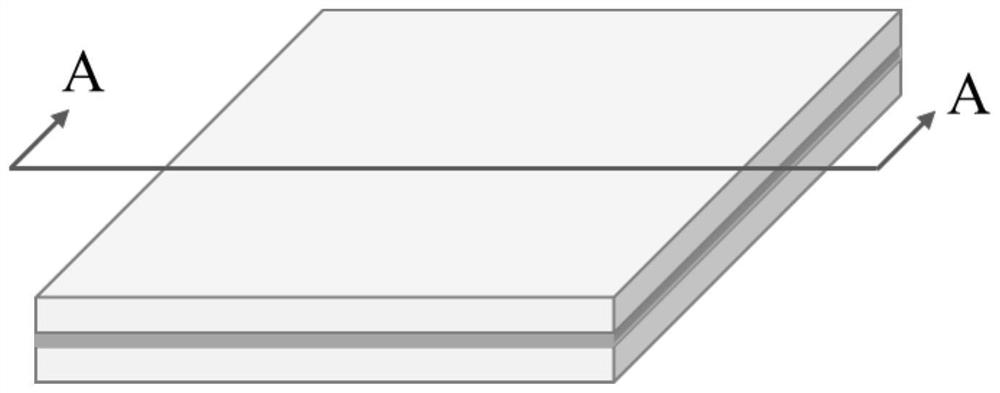
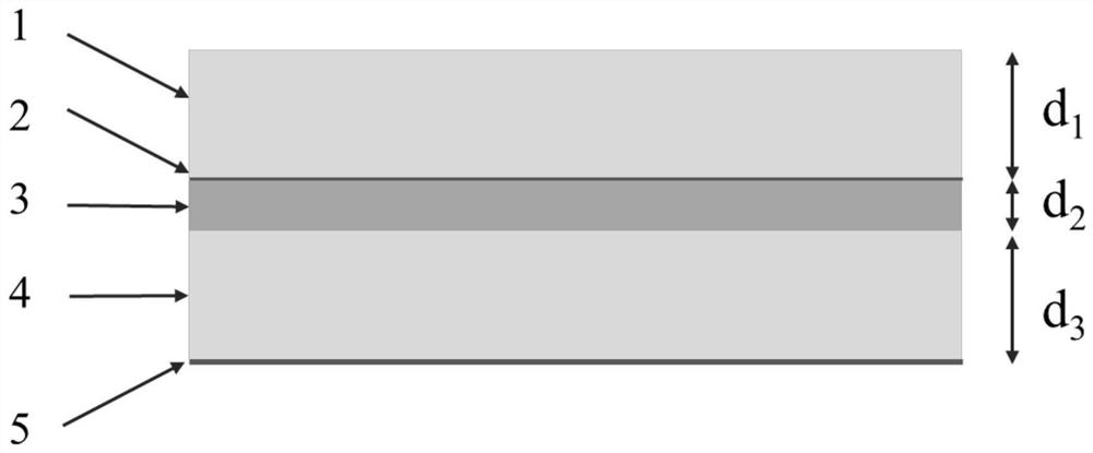
[0048] Such as figure 1 , 2 A broadband transparent absorbing material based on a double-layer conductive film is shown, including a first transparent medium layer and a third transparent medium layer, a first transparent conductive film and a second transparent conductive film, and a second transparent medium layer in the middle . External incident electromagnetic waves act on the designed wave-absorbing material from the first transparent medium layer, and both the first conductive film and the second conductive film are located on the side of the transparent medium substrate away from the incident wave.
[0049] In this embodiment, for the selection of materials, the first transparent medium layer is made of high boron glass, the second transparent medium layer is made of soda lime glass, the bonding material is SGP, and the transparent conductive material is ITO. It should be understood that, for the broadband absorbing material based on the double-layer transparent cond...
Embodiment 2
[0053] Embodiment 2 has the same structure as Embodiment 1, only the following parameters have been adjusted:
[0054] The third transparent medium layer is made of high boron glass, the dielectric constant is 4.8*(1-j0.003), and the thickness d of the third transparent medium layer 3 3mm.
[0055] Figure 5 It is the reflection characteristic curve of the broadband transparent absorbing material based on the double-layer transparent conductive film corresponding to Example 2 of the present invention. It can be seen that the reflections in the 5.2-15.2GHz frequency band are all lower than -10dB. Figure 6 It is the transmission characteristic curve of the broadband transparent absorbing material based on the double-layer conductive film corresponding to Example 2 of the present invention. It can be seen that the transmission in the 0-18GHz frequency band is all lower than -24dB.
Embodiment 3
[0057] Embodiment 3 has the same structure as Embodiment 1, only the following parameters have been adjusted:
[0058] The first transparent medium layer adopts polymethyl methacrylate, its dielectric constant is 3.0*(1-j0.003), the thickness d of the first transparent medium layer 1 is 3.7mm. Thickness d of the second transparent medium layer 2 is 1.3mm. The third transparent medium layer adopts polymethyl methacrylate, its dielectric constant is 3.0*(1-j0.003), the thickness d of the third transparent medium layer 3 is 2.3mm. The transparent conductive material used for the conductive film layer is FTO.
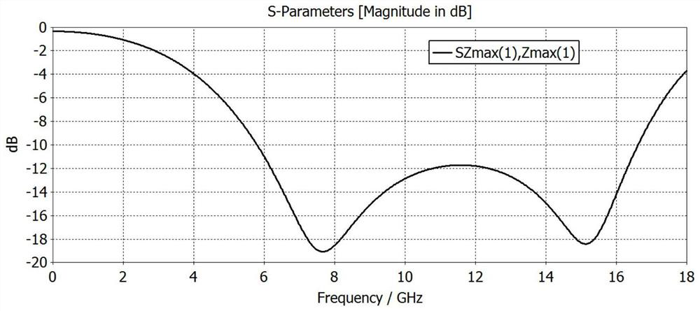
[0059] Figure 7 It is the reflection characteristic curve of the broadband transparent absorbing material based on the double-layer conductive film corresponding to Example 3 of the present invention. It can be seen that the reflection in the 6.0-17.7GHz frequency band is all lower than -10dB, and the reflection in the 7.7-15.8GHz frequency band is lower than -10dB. ...
PUM
| Property | Measurement | Unit |
|---|---|---|
| Square resistance | aaaaa | aaaaa |
| Thickness | aaaaa | aaaaa |
| Thickness | aaaaa | aaaaa |
Abstract
Description
Claims
Application Information
 - R&D
- Intellectual Property
- Life Sciences
- Materials
- Tech Scout
- Unparalleled Data Quality
- Higher Quality Content
- 60% Fewer Hallucinations
Browse by: Latest US Patents, China's latest patents, Technical Efficacy Thesaurus, Application Domain, Technology Topic, Popular Technical Reports.
© 2025 PatSnap. All rights reserved.Legal|Privacy policy|Modern Slavery Act Transparency Statement|Sitemap|About US| Contact US: help@patsnap.com