Manufacturing method of display substrate, display substrate and display device

A technology for display substrates and manufacturing methods, which is applied in semiconductor/solid-state device manufacturing, electrical components, electric solid-state devices, etc., and can solve problems such as dark spots and isolation failures in display panels

Pending Publication Date: 2020-09-11
BOE TECH GRP CO LTD +1
View PDF5 Cites 8 Cited by
  • Summary
  • Abstract
  • Description
  • Claims
  • Application Information

AI Technical Summary

Problems solved by technology

[0005] The present invention provides a method for manufacturing a display substrate, a display substrate and a display device, so as to solve the problems in the prior art that the use of SD isolation columns is likely to cause dark spots on the display panel and lead to isolation failure

Method used


Image

  • Manufacturing method of display substrate, display substrate and display device
  • Manufacturing method of display substrate, display substrate and display device
  • Manufacturing method of display substrate, display substrate and display device

Examples


Embodiment 1

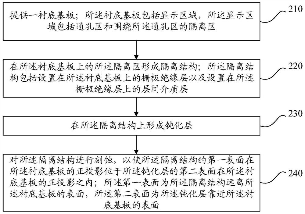
[0067] refer to figure 2 , which shows a flow chart of a method for manufacturing a display substrate according to Embodiment 1 of the present invention, which may specifically include the following steps:

[0068] Step 210, providing a base substrate; the base substrate includes a display area, and the display area includes a via area and an isolation area surrounding the via area.

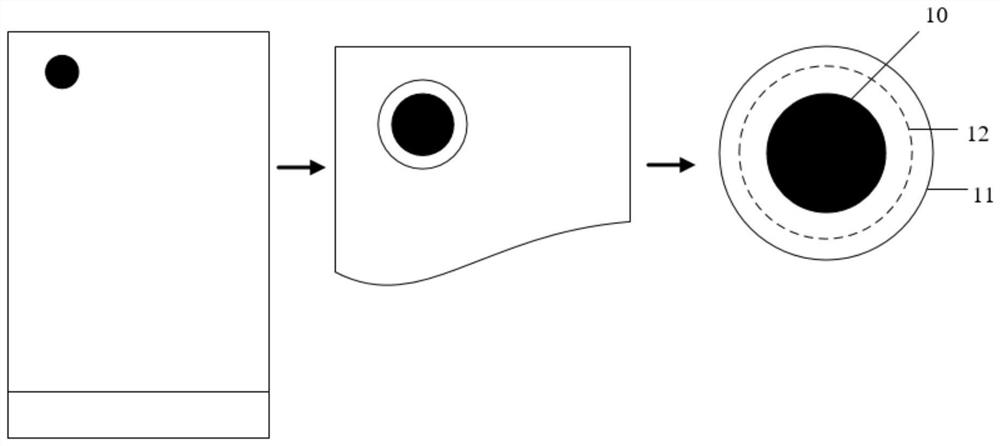
[0069] In an embodiment of the present invention, a base substrate is provided, the base substrate includes a display area, and the display area includes a through-hole area 10 and an isolation area 11 surrounding the through-hole area 10, such as image 3 As shown, it is a schematic plan view of a display panel formed by using the display substrate of the embodiment of the present invention. The through-hole area 10 in the display substrate refers to the display panel formed by the display substrate for installing a camera or an infrared scanning device. and other functional device areas, the ...

Embodiment 2

[0108] Embodiment 2 of the present invention provides a display substrate, including:

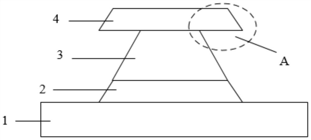
[0109] The base substrate 20, the base substrate 20 includes a display area, and the display area includes a through hole area 10 and an isolation area 11 surrounding the through hole area 10;

[0110] The isolation structure 30 of the isolation region 11 formed on the base substrate 20, the isolation structure 30 includes a gate insulating layer 103 disposed on the base substrate 20 and an interlayer dielectric layer 104 disposed on the gate insulating layer;

[0111] a passivation layer 105 formed on the isolation structure 30;

[0112] Wherein, the orthographic projection of the first surface of the isolation structure 30 on the base substrate 20 is located within the orthographic projection of the second surface of the passivation layer 105 on the base substrate 20; The second surface is the surface of the passivation layer 105 close to the base substrate 20 .

[0113] The display sub...


PUM


Abstract

The invention provides a manufacturing method of a display substrate, the display substrate and a display device, and relates to the technical field of display. According to the embodiment of the invention, a substrate is provided. The substrate comprises a display area, and the display area comprises a through hole area and an isolation area surrounding the through hole area. An isolation structure is formed on the isolation area on the substrate; the isolation structure comprises a gate insulating layer arranged on the substrate and an interlayer dielectric layer arranged on the gate insulating layer. A passivation layer on the isolation structure; the isolation structure is etched, so that the orthographic projection of the first surface, far away from the substrate, of the isolation structure on the substrate is located in the orthographic projection of the second surface, close to the substrate, of the passivation layer on the substrate; therefore, the contact position of the passivation layer and the isolation structure is disconnected when an organic material is evaporated, water and oxygen in the through hole area are prevented from being transmitted to other areas in the display area through the organic material, and the problem of isolation failure when a metal isolation structure is adopted is also solved.

Description

technical field [0001] The invention relates to the field of display technology, in particular to a method for manufacturing a display substrate, a display substrate and a display device. Background technique [0002] For existing flexible AMOLED (Active-matrix organic light emitting diode, active-matrix organic light-emitting diode) products, it has become a popular way to set the front camera or infrared scanning device inside the display area in order to achieve a larger screen ratio. At this time, it is necessary to form a through hole in the display area, and then install the front camera or infrared scanning device at the position corresponding to the through hole. Since the completion of the through hole is carried out in the module process stage, after the through hole is formed, The organic material evaporated at the edge will be exposed, thereby forming a water and oxygen erosion path, causing the problem of poor black spots in the effective display area of ​​the d...

Claims


Application Information

Patent Timeline
Patent Type & Authority Applications(China)
IPC IPC(8): H01L21/77H01L27/12H01L27/32H01L51/52
CPCH01L27/1218H01L27/1288H10K59/12H10K50/8428H10K50/844
Inventor 王文涛史大为王培杨璐段岑鸿赵天龙吴广鑫王玲玲赵东升司晓文
Owner BOE TECH GRP CO LTD
Why Eureka
Try Eureka