Super junction surface metal oxide semiconductor field effect transistor structure
An oxide semiconductor and field effect transistor technology, applied in the field of super junction metal oxide semiconductor field effect transistor structure, can solve the problems of circuit board damage, economic loss, explosion of super junction transistor, etc., and achieves safe and convenient use and structure. scientifically sound effects
- Summary
- Abstract
- Description
- Claims
- Application Information
AI Technical Summary
Problems solved by technology
Method used
Image
Examples
Embodiment 1
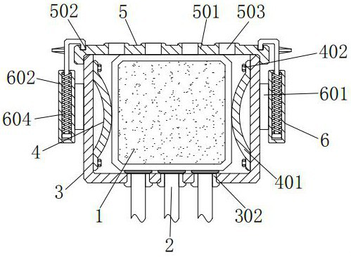
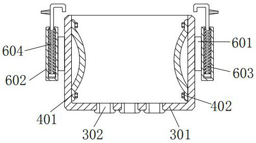
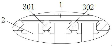
[0035] A super junction metal oxide semiconductor field effect transistor structure, comprising a super junction metal oxide semiconductor field effect transistor 1, a plurality of output terminals 2 are installed on the bottom of the super junction metal oxide semiconductor field effect transistor 1, the super junction The outer wall of the metal oxide semiconductor field effect transistor 1 is provided with a protection mechanism 3, the protection mechanism 3 includes a box body 301 and a first through hole 302, the inner wall of the box body 301 and the outer wall of the super junction metal oxide semiconductor field effect transistor 1 fit together, so that the super junction metal oxide semiconductor field effect transistor 1 can be placed on the inner wall of the box body 301, the bottom of the box body 301 is processed with a plurality of first through holes 302, and the inner walls of the plurality of first through holes 302 are respectively The gap fits with the outer ...
Embodiment 2
[0037] As an option, see Figure 1-4 , super junction metal oxide semiconductor field effect transistor structure, the left and right sides of the inner wall of the box body 301 are provided with a fixing mechanism 4, the fixing mechanism 4 includes an elastic piece 401 and a bolt 402. Two elastic pieces 401 are respectively arranged on the sides of the box body 301 On the left and right sides of the inner wall, two elastic sheets 401 are respectively threadedly connected to the left and right sides of the inner wall of the box body 301 through a plurality of bolts 402, and the inner sides of the two elastic sheets 401 are offset against the outer wall of the super junction metal oxide semiconductor field effect transistor 1 Tight, so that the super junction metal oxide semiconductor field effect transistor 1 can be fixed on the inner wall of the box body 301 through the elastic sheet 401, and the two elastic sheets 401 are symmetrically distributed about the super junction met...
Embodiment 3
[0040] As an option, see figure 1 , 5 And 6, super junction metal oxide semiconductor field effect transistor structure, the top of box body 301 is provided with heat dissipation mechanism 5, and heat dissipation mechanism 5 comprises box body cover 501, card groove 502 and second through hole 503, and box body cover 501 The inner wall is matched with the top of the outer wall of the box body 301 in clearance, and the top left and right sides of the box body cover 501 are fixedly connected with card slots 502, and the top of the box body cover 301 is processed with a plurality of second through holes 503, and the second through holes 503 are used In order to dissipate and dissipate the heat generated by the super junction metal oxide semiconductor field effect transistor 1, the gap between the inner wall of the box cover 501 and the outer wall of the box body 301 is 0.5-1 mm, so that the box cover 501 can be stably reconciled in the box body On the outer wall of 301 , the sec...
PUM
 Abstract
Description
Claims
Application Information


