Defect identification method of semiconductor laser

A defect identification and semiconductor technology, applied in the direction of material capacitance, etc., can solve problems such as semiconductor laser damage

Active Publication Date: 2020-09-18
SUZHOU INST OF NANO TECH & NANO BIONICS CHINESE ACEDEMY OF SCI
View PDF14 Cites 0 Cited by
  • Summary
  • Abstract
  • Description
  • Claims
  • Application Information

AI Technical Summary

Problems solved by technology

In the production of semiconductor lasers, a large number of defects will be generated during the production process of growing semiconductor materials.
[0003] The traditional method of defect identification in semiconductor lasers can only identify defects on the surface of semiconductor materials. If it is necessary to identify defects inside the semiconductor material, the only way to identify defects is to choose a cutting method with permanent damage after cutting the semiconductor material. However, this usually Will cause permanent damage to the semiconductor laser

Method used


Image

  • Defect identification method of semiconductor laser
  • Defect identification method of semiconductor laser
  • Defect identification method of semiconductor laser

Examples


Embodiment Construction

[0023] Hereinafter, embodiments of the present invention will be described in detail with reference to the accompanying drawings. This invention may, however, be embodied in many different forms and should not be construed as limited to the specific embodiments set forth herein. Rather, the embodiments are provided to explain the principles of the invention and its practical application, thereby enabling others skilled in the art to understand the invention for various embodiments and with various modifications as are suited to particular intended uses.

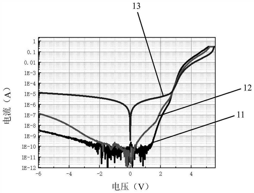
[0024] figure 1 is a voltage-current graph of a semiconductor laser according to an embodiment of the present invention. refer to figure 1 , which shows three curves, respectively the first curve 11 corresponding to the semiconductor laser not aging, the second curve 12 corresponding to the semiconductor laser in the first aging stage, and the corresponding first curve 12 when the semiconductor laser is in the second aging ...


PUM


Abstract

The invention provides a defect identification method of a semiconductor laser. The defect identification method comprises the following steps: acquiring a first relation curve graph of capacitance and frequency of a semiconductor laser in an aging process; and acquiring defect energy level information and / or defect distribution information of the semiconductor laser according to the first relation curve graph. The invention further provides another defect identification method of a semiconductor laser, which comprises the following steps: acquiring a second relation curve graph of the apparent carrier concentration and the depletion region width of a semiconductor laser in the aging process; and acquiring defect distribution information of the semiconductor laser according to the second relation curve graph. According to the invention, the defect identification of the semiconductor laser is carried out by adopting the electrical characteristics of the semiconductor laser, and the defect identification is carried out without adopting a cutting method with permanent damage to cut a semiconductor material, so that the defect of the semiconductor laser can be identified in a nondestructive manner, and the permanent damage to the semiconductor laser is avoided.

Description

technical field [0001] The invention belongs to the field of optoelectronic technology, and in particular relates to a defect identification method of a semiconductor laser capable of non-destructively identifying defects of the semiconductor laser. Background technique [0002] As an important semiconductor light-emitting device, semiconductor lasers have broad application prospects in the fields of laser display and laser lighting. In the manufacture of semiconductor lasers, a large number of defects will be generated during the production process such as growing semiconductor materials. [0003] The traditional method of defect identification in semiconductor lasers can only identify defects on the surface of semiconductor materials. If it is necessary to identify defects inside the semiconductor material, the only way to identify defects is to choose a cutting method with permanent damage after cutting the semiconductor material. However, this usually Will cause permane...

Claims


Application Information

Patent Timeline
Patent Type & Authority Applications(China)
IPC IPC(8): G01N27/24
CPCG01N27/24
Inventor 李德尧温鹏雁黄思溢张立群刘建平张书明杨辉
Owner SUZHOU INST OF NANO TECH & NANO BIONICS CHINESE ACEDEMY OF SCI
Why Eureka
Try Eureka