Compensation capacitor structure and capacitance value increasing method thereof

A technology for compensating capacitors and capacitors, which is applied in the OLED field, can solve problems such as breakdown, lower aperture ratio, and inability to reduce device size, etc., to achieve the effect of increasing capacitance, increasing aperture ratio, and improving display quality

Pending Publication Date: 2020-09-18
FUJIAN HUAJIACAI CO LTD
View PDF10 Cites 0 Cited by
  • Summary
  • Abstract
  • Description
  • Claims
  • Application Information

AI Technical Summary

Problems solved by technology

The method of increasing the storage capacitor is usually to increase the area of ​​the electrode plates and reduce the distance between the two electrode plates. However, increasing the area of ​​the electrode plates cannot reduce the size of the device and cause a decrease in the aperture ratio. Simply reducing the area of ​​the two electrode plates will be insulated Layer thickness limitation and risk of breakdown

Method used


Image

  • Compensation capacitor structure and capacitance value increasing method thereof
  • Compensation capacitor structure and capacitance value increasing method thereof

Examples


Embodiment 1

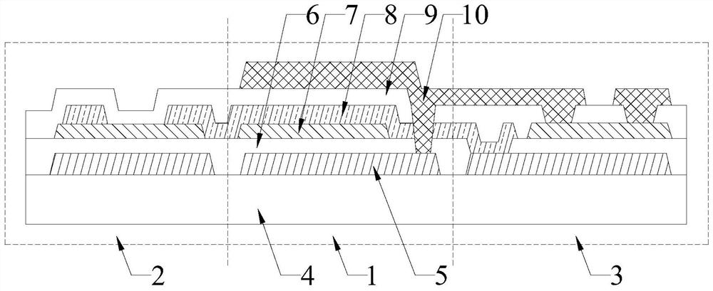
[0051] Please refer to figure 1 , Embodiment 1 of the present invention is:

[0052] A compensation capacitance structure, comprising a capacitance region structure 1, the capacitance region structure 1 comprising a glass layer 4, on the surface of the glass layer 4 of the capacitance region structure 1, a first metal layer 5 and a first insulating layer are sequentially laminated 6. A semiconductor layer 7, a second metal layer 8, a second insulating layer 9 and a third metal layer 10;

[0053] The first insulating layer 6 of the capacitive region structure 1 is provided with a first via hole, the second metal layer 8 of the capacitive region structure 1 is provided with a second via hole, and the second insulating layer of the capacitive region structure 1 Layer 9 is provided with a third via hole, the third via hole, the second via hole and the first via hole are oppositely arranged and communicated, and the third via hole, the second via hole and the first via hole are al...

Embodiment 2

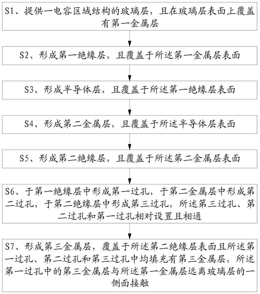
[0064] Please refer to figure 2 , the second embodiment of the present invention is:

[0065] A method for improving the capacitance of a compensation capacitor structure, comprising the following steps:

[0066] S1, providing a glass layer 4 of the capacitive region structure 1, and covering the surface of the glass layer 4 with a first metal layer 5;

[0067] S2, forming a first insulating layer 6 and covering the surface of the first metal layer 5;

[0068] S3, forming a semiconductor layer 7 and covering the surface of the first insulating layer 6;

[0069] S4, forming a second metal layer 8 and covering the surface of the semiconductor layer 7;

[0070] S5, forming a second insulating layer 9 and covering the surface of the second metal layer 8;

[0071] S6, forming a first via hole in the first insulating layer 6, forming a second via hole in the second metal layer 8, forming a third via hole in the second insulating layer 9, the third via hole, the second via hole ...


PUM

PropertyMeasurementUnit
thicknessaaaaaaaaaa

Abstract

The invention relates to the technical field of OLEDs, in particular to a compensation capacitor structure and a capacitance value increasing method thereof. A first metal layer, a first insulating layer, a semiconductor layer, a second metal layer, a second insulating layer and a third metal layer of a capacitance region structure are sequentially arranged on the surface of a glass layer of the capacitance region structure; a first capacitor is formed among the first metal layer, the first insulating layer and the semiconductor layer, and a second capacitor is formed among the second metal layer, the second insulating layer and the third metal layer, so that a parallel circuit structure is formed between the first capacitor and the second capacitor, and the capacitance value is increased.According to the compensation capacitor structure designed in the scheme, a photomask can be saved on the basis of an existing technological process, the uniformity of a panel picture is effectivelyimproved, the display quality is improved, the requirement for a smaller electrode plate area is met, and the effect of increasing the aperture opening ratio is achieved.

Description

technical field [0001] The invention relates to the technical field of OLEDs, in particular to a compensation capacitance structure and a method for increasing the capacitance thereof. Background technique [0002] With the development and progress of display technology, people put forward higher requirements for the quality of the display. At present, achieving higher resolution has become an inevitable trend of the display industry in the future. [0003] Organic Light Emitting Diode (OLED for short), the existing OLED devices generally have a 2T1C (two transistors sandwiching a storage capacitor) structure, and the storage capacitor is the main means to maintain the potential of the speed-limiting electrode, which increases the storage capacity uniformly. Capacitors can effectively improve the uniformity of the picture and enhance the display quality. The method of increasing the storage capacitor is usually to increase the area of ​​the electrode plates and reduce the d...

Claims


Application Information

Patent Timeline
Patent Type & Authority Applications(China)
IPC IPC(8): H01L27/32H01L49/02
CPCH01L28/40H10K59/1216H10K59/1201
Inventor 宋爽
Owner FUJIAN HUAJIACAI CO LTD
Why Eureka
Try Eureka