Display substrate and preparation method thereof, display panel and display device

A technology for display substrates and display panels, used in semiconductor/solid-state device manufacturing, diodes, semiconductor devices, etc., can solve the problems of small line width and line spacing of power supply lines, and achieve improved display uniformity, small power supply voltage difference, The effect of reducing pressure drop

Active Publication Date: 2020-09-18
BOE TECH GRP CO LTD +1
View PDF3 Cites 11 Cited by
  • Summary
  • Abstract
  • Description
  • Claims
  • Application Information

AI Technical Summary

Problems solved by technology

[0005] In view of the above problems, the purpose of the embodiments of the present invention is to provide a display substrate, a display panel, a display device, and a method for preparing a display substrate, so as to solve the problem of edge metal winding in the under-screen camera area in the prior art. The problem of the line width and line spacing of the existing power supply lines is small

Method used


Image

  • Display substrate and preparation method thereof, display panel and display device
  • Display substrate and preparation method thereof, display panel and display device
  • Display substrate and preparation method thereof, display panel and display device

Examples


preparation example Construction

[0050] refer to Figure 6 , the embodiment of the present invention also discloses a method for preparing a display substrate, including:

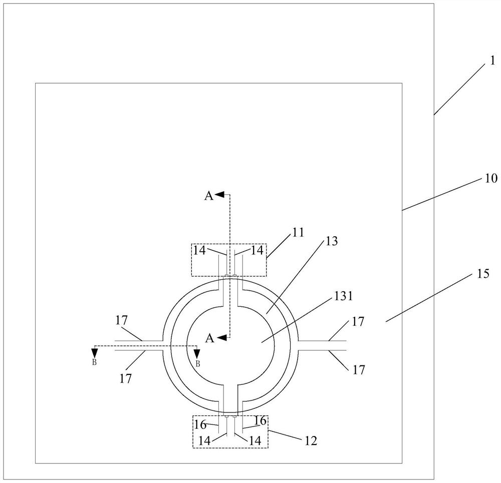
[0051] Step 610, providing a substrate corresponding to the display area. The substrate includes a first wiring area, a second wiring area, and an under-screen camera area. The under-screen camera area is located between the first wiring area and the second wiring area.

[0052] Step 620, forming an inorganic layer and a first power line on both the first wiring area and the second wiring area of ​​the substrate.

[0053] Step 630, forming an inorganic layer and a first flat layer on the under-screen camera area of ​​the substrate close to the first wiring area and the second wiring area, and forming a second flat layer on the first power line.

[0054] Step 640, forming an overlapping layer on the first power line between the first planar layer and the second planar layer.

[0055] Step 650 , forming a pixel defining layer on the overla...


PUM


Abstract

The invention provides a display substrate and a preparation method thereof, a display panel and a display device. A first wiring area, a second wiring area and an under-screen camera area are arranged in a display area of the display substrate. The under-screen camera area is located between the first wiring area and the second wiring area, a transparent cathode layer is arranged in the under-screen camera area, the transparent cathode layer is formed on a substrate of the display substrate, and the transparent cathode layer is electrically connected with a first power supply wiring of the first wiring area and a first power supply wiring of the second wiring area. According to the invention, a power supply signal of the display substrate can directly pass through the under-screen cameraarea; power supply wiring does not need to be wound in the edge of the under-screen camera area; the wiring width of the first power supply wiring of the first wiring area and the wiring width of thefirst power supply wiring of the second wiring area and the wiring distance between the first power supply wiring of the first wiring area and other wiring can be ensured, the power supply wiring voltage drop is reduced, the open circuit problem, the short circuit problem and the inter-wire crosstalk problem are solved, and the power supply voltage difference between the first wiring area and thesecond wiring area is small.

Description

technical field [0001] The present invention relates to the field of display technology, in particular to a display substrate, a display panel, a display device and a method for preparing a display substrate. Background technique [0002] With the popularization of full screens, the under-screen camera set in the display area has gradually become the mainstream. The display area corresponding to the under-screen camera is dug out to form the under-screen camera area, which has become a mainstream design. The under-screen camera area retains the luminous material layer and transparent Cathode layer, the product form of its full screen is as follows figure 1 as shown, figure 1 Among them, 1' is the camera area under the screen, 2' is the display area, 3' is the connection area, and 4' is the full screen. [0003] Such as figure 2 As shown, in the prior art, the gate drive control wiring 11', the data wiring 12' and the power wiring 13' are usually arranged by winding at th...

Claims


Application Information

Patent Timeline
Patent Type & Authority Applications(China)
IPC IPC(8): H01L27/32H01L21/77
CPCH10K59/65H10K59/131H10K59/1201
Inventor 张云鹏陈珍祥
Owner BOE TECH GRP CO LTD
Why Eureka
Try Eureka