Low-temperature test structure of multi-channel high-frequency chip

A low-temperature test, multi-channel technology, applied in the direction of electronic circuit testing, measuring electricity, measuring devices, etc., can solve the problems of not using high frequency, the distance between test points can not be too small, high frequency impedance mismatch, etc., to achieve convenient disassembly and assembly Effect

Pending Publication Date: 2020-09-22
SHANGHAI INST OF MICROSYSTEM & INFORMATION TECH CHINESE ACAD OF SCI
View PDF13 Cites 0 Cited by
  • Summary
  • Abstract
  • Description
  • Claims
  • Application Information

AI Technical Summary

Problems solved by technology

[0004] The existing published patent publication number is CN104764909A, and the name is "convenient chip test seat that can be used for extremely low temperature measurement". It uses vertical metal pogo pins to realize the connection between the sample test point and the pad on the PCB circuit board. It has the following features: The disadvantages are: 1. The size of the metal pogo pin is limited (it cannot be processed too small, the minimum size is about φ0.4mm, and a certain gap is required between the pogo pins, at least 1mm), which limits the test point spacing of the sample chip that can be tested. Too small, the contact pad of the test point should not be too small, (the test point pad of the sample chip needs to be ≥0.4mm, and the pad spacing needs to be >1mm)
However, the pads of many integrated circuit chips will be less than φ0.4mm, and the pad spacing is even less than 1mm; 2. The metal pogo pin structure connected vertically up and down cannot be used for high frequencies, but only for low frequencies. The high-frequency impedance mismatch is serious, and the loss will very big

Method used


Image

  • Low-temperature test structure of multi-channel high-frequency chip
  • Low-temperature test structure of multi-channel high-frequency chip
  • Low-temperature test structure of multi-channel high-frequency chip

Examples


Embodiment Construction

[0021] The present invention will be further described below in conjunction with specific embodiments. It should be understood that these examples are only used to illustrate the present invention and not to limit the scope of the present invention. In addition, it should be understood that after reading the content taught by the present invention, those skilled in the art can make various changes or modifications to the present invention, and these equivalent forms also fall within the scope defined by the appended claims of the present application.

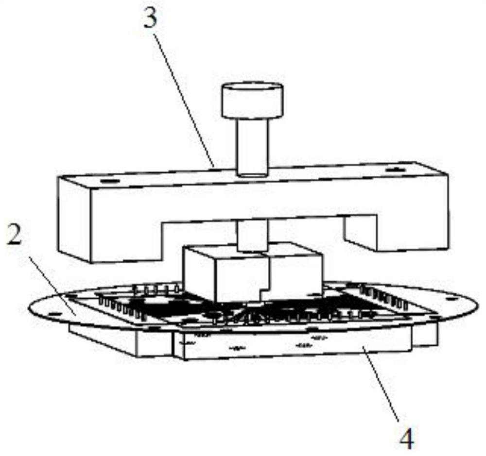
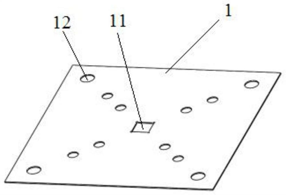
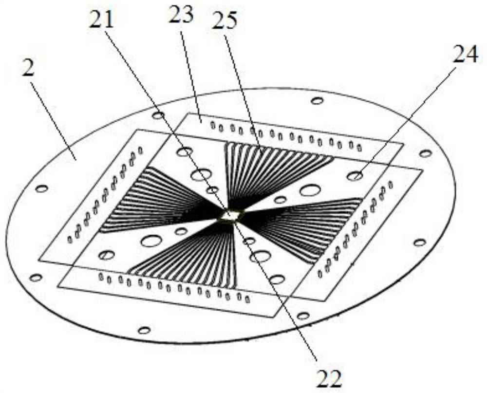
[0022] Embodiments of the present invention relate to a low-temperature test structure of a multi-channel high-frequency chip, such as figure 1 As shown, it includes a chip positioning printed circuit board 1, a multi-channel interface circuit board 2 and a pressure device 3. The chip positioning printed circuit board 1 is used to place the chip to be tested; the multi-channel interface circuit board 2 is provided with There ar...


PUM


Abstract

The invention relates to a low-temperature test structure of a multi-channel high-frequency chip. The structure comprises a chip positioning printed circuit board, a multi-channel interface circuit board and a pressure applying device. The chip positioning printed circuit board is used for placing a chip to be tested. The multi-channel interface circuit board is provided with a multi-channel metalprobe structure, and the metal probe structure is used for realizing signal input and output of a to-be-tested chip and external equipment. And the pressure applying device is used for applying pressure to enable a pin pad of a chip to be tested on the chip positioning printed circuit board to be in contact with the multiple paths of metal probes on the multi-channel interface circuit board so asto realize electrical connection. According to the invention, completeness and no damage of the chip in the test can be ensured.

Description

technical field [0001] The invention relates to the technical field of superconducting digital integrated circuit testing, in particular to a low-temperature testing structure of a multi-channel high-frequency chip. Background technique [0002] The future development of superconducting digital integrated circuits will require extensive testing using a large number of input / output (I / O) lines to apply independent bias control, input test signals and monitor the outputs of different subcircuits. There is an increasing demand for standardized test structures corresponding to various complex superconducting chips and multi-chip modules. Such a test structure must support multiple I / O lines, be easy and cost-effective to operate, and support long-term automated testing. In addition, in the superconducting integrated circuit chip development cycle, since the design infrastructure and manufacturing process of integrated circuits are relatively immature, it is usually necessary to...

Claims


Application Information

Patent Timeline
Patent Type & Authority Applications(China)
IPC IPC(8): G01R1/04G01R31/28
CPCG01R1/0416G01R31/2851G01R31/2877
Inventor 汪书娜李凌云余慧勤尤立星
Owner SHANGHAI INST OF MICROSYSTEM & INFORMATION TECH CHINESE ACAD OF SCI
Why Eureka
Try Eureka