Chip metal bump forming method

A metal bump and molding method technology, which is applied in the manufacturing of electrical components, electric solid-state devices, semiconductor/solid-state devices, etc. The effect of repairing damage

Inactive Publication Date: 2020-09-29
CHIPMORE TECH CORP LTD +1
View PDF4 Cites 0 Cited by
  • Summary
  • Abstract
  • Description
  • Claims
  • Application Information

AI Technical Summary

Problems solved by technology

But when doing CP testing, the probe needs to be in contact with the metal cap of the metal bump, which may cause damage to the metal cap to form test

Method used


Image

  • Chip metal bump forming method
  • Chip metal bump forming method
  • Chip metal bump forming method

Examples


Embodiment Construction

[0038] The embodiments described below by referring to the figures are exemplary only for explaining the present invention and should not be construed as limiting the present invention.

[0039] Embodiments of the present invention: as figure 1 As shown, a chip metal bump forming method is disclosed, comprising the steps of:

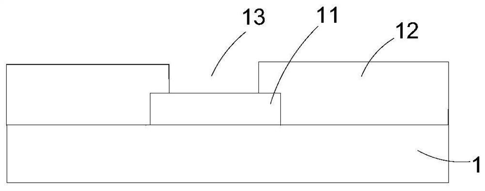
[0040] Step 101 : providing a silicon substrate 1 , an electrode 11 and a passivation layer 12 are formed on the upper surface of the silicon substrate 1 , and the electrode 11 is exposed from a passivation layer opening 13 on the passivation layer 12 . An electrode 11 is formed on the silicon substrate 1, a passivation layer 12 covers the silicon substrate 1 and part of the electrode 11, the passivation layer 12 overlaps the edge position of the part of the electrode 11, and the area of ​​the electrode 11 not covered by the passivation layer 12 exposed outwards to form passivation layer openings 13, such as figure 2 shown.

[0041] S103: if image ...


PUM

PropertyMeasurementUnit
Wavelengthaaaaaaaaaa

Abstract

The invention discloses a chip metal bump forming method, the method comprises the following steps of providing a silicon substrate, forming an electrode and a passivation layer on the upper surface of the silicon substrate, and exposing an electrode outwards from an opening of the passivation layer in the passivation layer; covering the upper surfaces of the passivation layer and the electrode with a seed layer; forming a photoresist layer on the upper surface of the seed layer; removing part of photoresist to form a photoresist opening which completely covers the area where the passivation layer opening is located; forming a metal column in the photoresist opening, wherein the metal column comprises a metal base layer and a metal tin layer which are sequentially formed from bottom to top; carrying out a chip probe test on the formed metal column; and forming a metal cap on the metal tin layer subjected to the chip probe test by adopting a reflux process. According to the method, thedamage to the end of the metal column in the chip probe testing process can be effectively repaired, needle marks formed in the chip probe testing process are rubbed down, therefore, the situation that the surfaces of the metal protruding blocks are uneven due to the needle marks is avoided, and then influences on the subsequent process and product performance are avoided.

Description

technical field [0001] The invention relates to the technical field of chip packaging, in particular to a chip metal bump forming method. Background technique [0002] In the process of semiconductor packaging, it is necessary to prepare bumps on the pad area of ​​the wafer first, then thin the crystal back to a certain thickness and cut it into individual chips, and finally connect the metal bumps on the chip to the solder pads on the substrate. pin binding. The fabrication and molding of metal bumps is a key technology in chip manufacturing and packaging. [0003] The fabrication of metal bumps generally ends with reflow soldering the tin pillars on top of the metal bumps to form a metal cap. In order to ensure a relatively stable yield rate of the bump manufacturing process and to save packaging costs, chip probe testing (CP, chip probing) is usually performed after the metal bumps are formed to screen the wafers and pick out unqualified chips. But when performing CP t...

Claims


Application Information

Patent Timeline
IPC IPC(8): H01L21/60
CPCH01L24/03H01L24/11H01L2224/0361H01L2224/0362H01L2224/03622H01L2224/03849H01L2224/11618H01L2224/11622H01L2224/11825H01L2224/11849H01L2224/11
Inventor 梅嬿陈浩
Owner CHIPMORE TECH CORP LTD
Why Eureka
Try Eureka