
Test circuit and chip

A technology for testing circuits and testing circuits, applied in circuits, printed circuit testing, electronic circuit testing, etc., can solve the problems of lack of chip protection, weak versatility, lack of strong versatility, etc., to achieve high market application value and improve versatility Effect

Pending Publication Date: 2020-10-09
XINBAI MICROELECTRONICS BEIJING
View PDF9 Cites 2 Cited by
  • Summary
  • Abstract
  • Description
  • Claims
  • Application Information

AI Technical Summary

Problems solved by technology

[0007] In other words, all tests must be based on the chip, whether the chip is still on the wafer or the chip has been packaged. However, all tests have the problems of strong specificity and weak universality, and lack of universality. Strong, also lacks a separate important test for special structures or functions, and lacks the protection of the chip before testing

Method used


Image

  • Test circuit and chip
  • Test circuit and chip
  • Test circuit and chip

Examples


Embodiment Construction

[0029] In order to facilitate the understanding of the present invention, the present invention will be described in more detail below in conjunction with the accompanying drawings and specific embodiments. However, the present invention can be implemented in many different forms and is not limited to the embodiments described in this specification. It should be noted that when an element is referred to as being “fixed” to another element, it can be directly on the other element or there can also be an intervening element. When an element is referred to as being "connected to" another element, it can be directly connected to the other element or intervening elements may also be present.

[0030] Unless otherwise defined, all technical and scientific terms used in this specification have the same meaning as commonly understood by one of ordinary skill in the technical field of the invention. The terms used in the description of the present invention in this specification are o...


PUM


Abstract

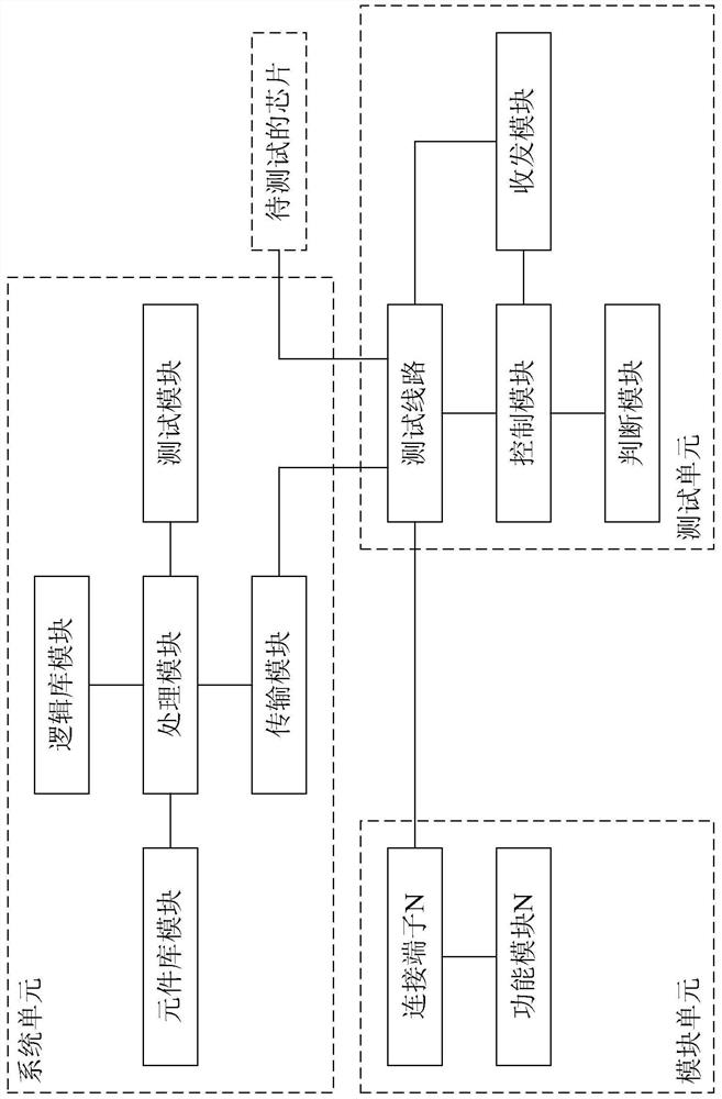
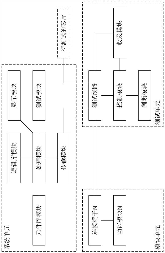
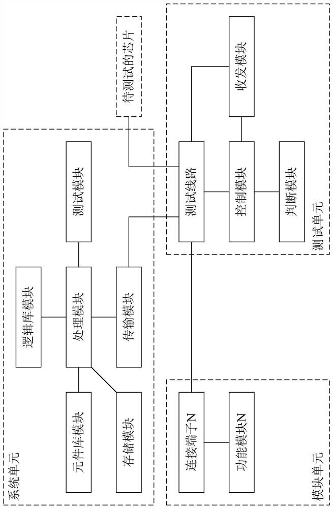
The invention discloses a test circuit and a chip. The test circuit comprises a system unit and a test unit. A control module sends test information to a transmission module through a transceiver module; a processing module receives the test information through the transmission module, calls a component library module and a logic library module to generate an analog circuit, calls the test moduleto test the analog circuit to obtain an analog test result, and feeds back the analog test result to the control module through the transmission module; and when it is determined that the simulation test result is normal, the to-be-tested chip is connected through the test circuit, and the chip is tested according to the test information. The control module is connected with a chip to be tested through a test circuit, the universality of the chip test is improved through cooperation, the analog circuit is generated through cooperation, and simulation can be performed before the test so that the chip is protected before the test, the damage to the chip caused by the test is avoided, and the test information can be adopted to perform independent test on the special structure or function of the chip.

Description

technical field [0001] The invention relates to the field of chips, in particular to a test circuit and a chip. Background technique [0002] With the development of technology, the application of chips has become ubiquitous, providing many supports for smart life and work, but chip testing is a relatively big problem, which directly runs through the entire process of chip design and mass production, whether it is tape-out Whether the final wafer test (Wafer Test) or the final test after packaging (Final Test, also known as packaging test) or the final system-level test requires one, two or multiple tests, especially the wafer test , its test object is a large number of chips on the wafer, these chips are bare chips (Die), they can be the same or different, the pin (Pin) after the bare chip is not packaged is the end user The pins seen, only the silicon chip pins (Pads) that are finally packaged inside the chip, will be connected by wires between the Pad and the Pin during ...

Claims


Application Information

Patent Timeline
IPC IPC(8): G01R31/28H01L21/66
CPCG01R31/2801H01L22/20
Inventor 杜占坤吕循洪
Owner XINBAI MICROELECTRONICS BEIJING
Learn More