Multi-die FPGA for balancing delay by utilizing active silicon connection layer

A technology that balances delay and connection layers, and is applied in CAD circuit design, special data processing applications, etc. It can solve the problems that it is difficult to meet the complex circuit requirements of large-scale integrated circuits, the structural limitations are large, and the device signal delay is difficult to design and adjust. , to achieve the effect of increasing Schmidt trigger characteristics, reducing processing difficulty, and reducing noise interference

Active Publication Date: 2020-10-09
WUXI ESIONTECH CO LTD
View PDF6 Cites 2 Cited by
  • Summary
  • Abstract
  • Description
  • Claims
  • Application Information

AI Technical Summary

Problems solved by technology

However, the above two patents are limited by the defects of the chip itself and the structural design. Both of them can only interconnect two adjacent IC dies arranged side by side, and can only realize signal interconnection in a single direction. The limitations are very large, and due to the limitations of the structure, the signal delay of the device is difficult to design and adjust, and it is actually difficult to meet the complex circuit requirements of large-scale integrated circuits

Method used


Image

  • Multi-die FPGA for balancing delay by utilizing active silicon connection layer
  • Multi-die FPGA for balancing delay by utilizing active silicon connection layer
  • Multi-die FPGA for balancing delay by utilizing active silicon connection layer

Examples


Embodiment Construction

[0049] The specific embodiments of the present invention will be further described below in conjunction with the drawings.

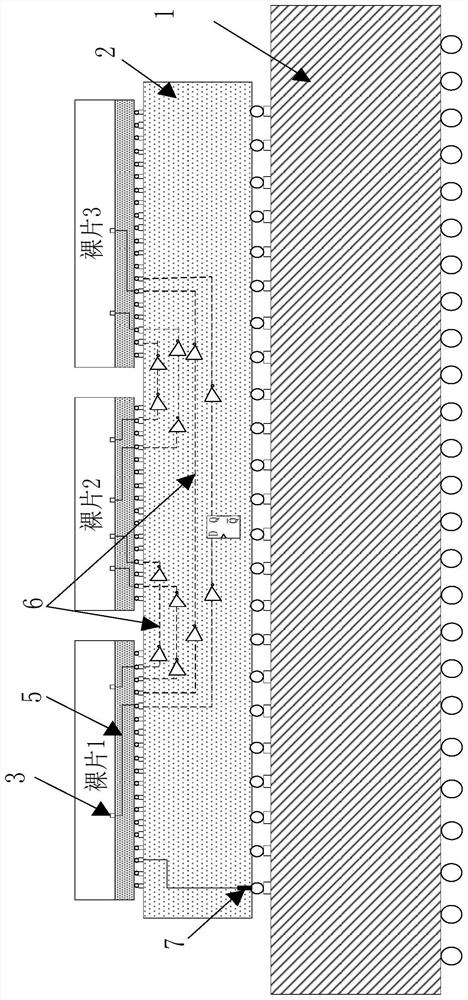
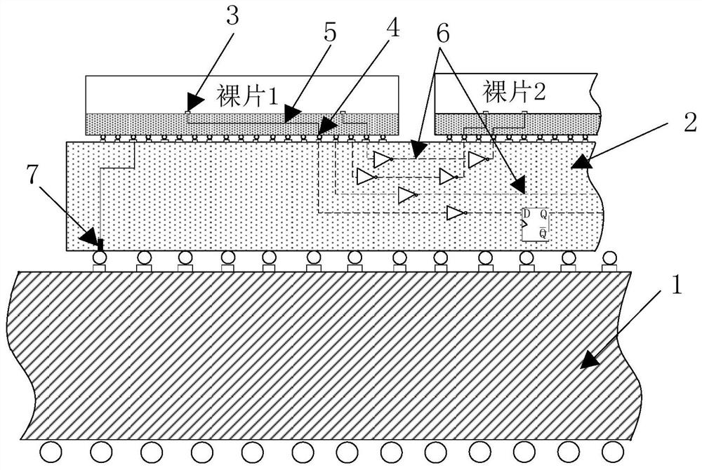
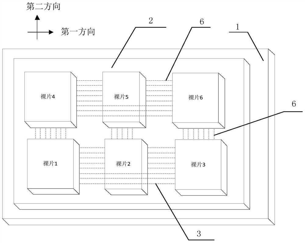
[0050] This application provides a multi-die FPGA that uses active silicon connection layers to balance delays, figure 1 Is a schematic cross-sectional view of the FPGA packaging structure of the present application, figure 2 Yes figure 1 An enlarged view of the middle part of the structure, image 3 Yes figure 1 The corresponding top view. The FPGA includes a substrate 1, a silicon connection layer 2 and a number of FPGA dies stacked in sequence from bottom to top. Figure 1-3 The structure shown includes 6 FPGA dies, denoted as dies 1-6 respectively. In actual implementation, the FPGA also includes a package shell for protecting each component that is packaged on the substrate 1, the silicon connection layer 2 and the FPGA die, and also includes pins connected to the substrate for signal extraction. figure 1 with 2 These conventional structures are not s...


PUM


Abstract

The invention discloses a multi-die FPGA for balancing the delay by utilizing an active silicon connection layer and relates to the technical field of FPGA. The multi-die FPGA comprises a substrate, asilicon connection layer on the substrate and a plurality of FPGA dies which are arranged on the silicon connection layer in a two-dimensional stacking mode in a stacked mode. The built-in silicon stack connection points of the FPGA dies are connected to the connection point leading-out ends, the connection point leading-out ends can be connected to other dies through cross-die connection lines in two directions in the active silicon connection layer, and two-dimensional interconnection communication between the dies is achieved. The active device arranged in the silicon connection layer canflexibly adjust the time delay of the cross-chip signal; the multi-die FPGA cross-chip signal time delay balance is realized, the time sequence convergence of the design is accelerated, the cascade structure supports the realization of large-scale and large-area FPGA products by cascading a plurality of small-scale and small-area dies, the processing difficulty is reduced, and the chip productionyield is improved.

Description

Technical field [0001] The invention relates to the field of semiconductor technology, in particular to a multi-die FPGA that utilizes active silicon connection layers to balance delays. Background technique [0002] FPGA (Field Programmable Gate Array, Field Programmable Gate Array) is a hardware programmable logic device. In addition to being used in mobile communications, data centers and other fields, it is also widely used in prototype verification in integrated circuit design and can be effectively verified. The correctness of the circuit function, while speeding up the circuit design speed. Prototype verification needs to use the programmable logic resources inside the FPGA to realize circuit design. With the continuous increase in the scale of integrated circuits and the realization of complex functions, the demand for the number of programmable logic resources in the FPGA continues to increase, and subsequent technological development and demand With the continuous incr...

Claims


Application Information

Patent Timeline
Patent Type & Authority Applications(China)
IPC IPC(8): G06F30/34
CPCG06F30/34
Inventor 单悦尔徐彦峰范继聪张艳飞闫华
Owner WUXI ESIONTECH CO LTD
Why Eureka
Try Eureka