Display panel and manufacturing method thereof and display device

A display panel and display area technology, which is applied in the fields of final product manufacturing, sustainable manufacturing/processing, semiconductor/solid-state device manufacturing, etc., and can solve problems such as the inability to realize a full screen

Active Publication Date: 2020-10-16
BOE TECH GRP CO LTD +1
View PDF5 Cites 15 Cited by
  • Summary
  • Abstract
  • Description
  • Claims
  • Application Information

AI Technical Summary

Problems solved by technology

[0005] The present invention provides a display panel, a manufacturing method thereof, and a display device, so as to solve the problem that the...

Method used


Image

  • Display panel and manufacturing method thereof and display device
  • Display panel and manufacturing method thereof and display device
  • Display panel and manufacturing method thereof and display device

Examples


Embodiment 1

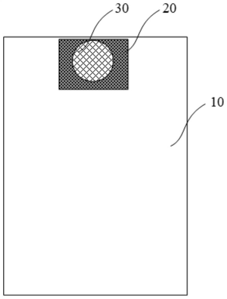
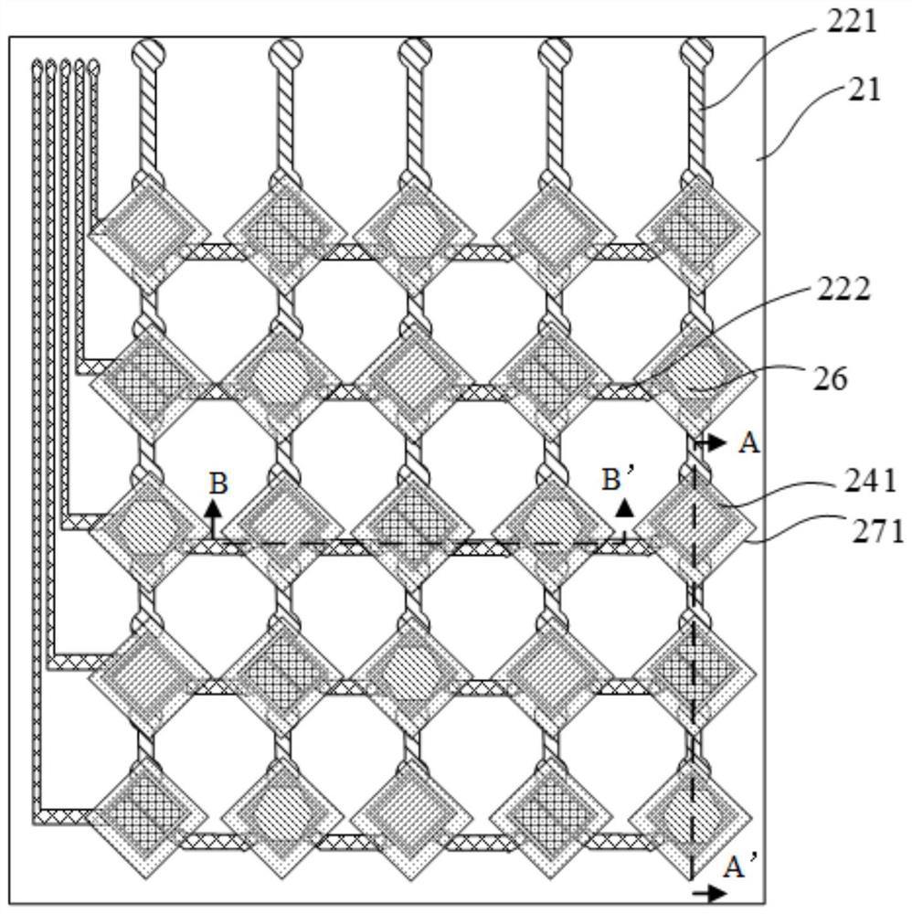
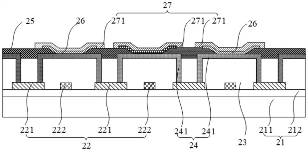
[0053] refer to figure 1 , showing a schematic diagram of a display panel according to an embodiment of the present invention, figure 2 shows a planar structure diagram of a functional display area in a display panel according to an embodiment of the present invention, image 3 show figure 2 A cross-sectional view of the shown display panel along section A-A', Figure 4 show figure 2 The shown display panel is a cross-sectional view along section B-B'.

[0054] The embodiment of the present invention provides a display panel, including: a substrate 21, the substrate 21 is divided into the effective display area 10 and the functional display area 20 where the functional device 30 is located; The electrode connection layer 22, the electrode connection layer 22 includes a plurality of mutually insulated anode connection lines 221 and cathode connection lines 222, and the anode connection lines 221 are distributed along the first direction, and the cathode connection lines ...

Embodiment 2

[0098] refer to Figure 6 , which shows a flow chart of a method for manufacturing a display panel according to an embodiment of the present invention, which may specifically include the following steps:

[0099] Step 601, providing a substrate; the substrate is divided into an effective display area and a functional display area where functional devices are located.

[0100]In the embodiment of the present invention, first, a substrate 21 is fabricated, and the substrate 21 is divided into an effective display area 10 and a functional display area 20 where the functional device 30 is located.

[0101] Specifically, an active layer, a gate insulating layer, and a gate layer are respectively formed on the effective display area 10 of the substrate 211, and then an interlayer dielectric layer is formed on both the effective display area 10 and the functional display area 20, and then, in the effective display area A source-drain electrode layer is formed on the interlayer diele...

Embodiment 3

[0128] An embodiment of the present invention provides a display device, including a functional device 30 and the above-mentioned display panel;

[0129] Wherein, the functional device 30 includes devices such as a camera and a sensor.

[0130] For the specific description of the display panel, reference may be made to the descriptions of Embodiment 1 and Embodiment 2, which will not be repeated in this embodiment of the present invention.

[0131] In addition, the display device also includes devices such as a driver chip and a TCON (Timer Control Register, timing controller).

[0132] In practical applications, the display device may be any product or component with a display function such as a mobile phone, a tablet computer, a monitor, a notebook computer, or a navigator.

[0133] In the embodiment of the present invention, the electrode connection layer, flat layer, anode layer, pixel defining layer, organic functional layer and cathode layer are sequentially arranged in...


PUM


Abstract

The invention provides a display panel and a manufacturing method thereof and a display device, and relates to the technical field of display. An electrode connecting layer, a flat layer, an anode layer, a pixel defining layer, an organic functional layer and a cathode layer are sequentially arranged on a substrate of a functional display area, the electrode connecting layer comprises a pluralityof anode connecting wires and cathode connecting wires which are insulated from one another; the anode layer comprises a plurality of anodes which are arranged at intervals, two adjacent anodes are connected with the anode connecting line through a first via hole penetrating through the flat layer, the cathode layer comprises a plurality of cathodes which are arranged at intervals, and two adjacent cathodes are connected with the cathode connecting line through a second via hole penetrating through the pixel defining layer and the flat layer. Due to the fact that the number of film layers of the function display area is small, the light transmittance can be improved, due to the fact that the number of wires of the function display area is small and the anodes and the cathodes are distributed at intervals, the light transmitting area of the function display area can be increased, the diffraction coherent superposition phenomenon is reduced, normal use of a function device is guaranteed,and full-screen display is achieved.

Description

technical field [0001] The present invention relates to the field of display technology, in particular to a display panel, a manufacturing method thereof, and a display device. Background technique [0002] With the continuous development of display technology, in order to provide users with a better visual experience, the full-screen design of the display device has become a trend and has been favored by more users. [0003] In the current display device, due to the need to install functional devices such as cameras and sensors, it is often necessary to cut and form accommodating grooves in the display device to place functional devices, such as notch screens and water drop screens in existing display devices. [0004] However, the current display device needs to form an accommodating groove to place functional devices, and the accommodating groove will occupy a part of the screen. Therefore, the screen ratio of the current display device cannot reach 100%, and a true full ...

Claims


Application Information

Patent Timeline
IPC IPC(8): H01L27/12H01L27/32H01L51/52H01L51/56
CPCH01L27/124H10K59/131H10K50/805H10K50/85H10K71/00Y02P70/50
Inventor 李杰张伟孙世成赵东升崔国意徐鲁陈腾卢玉群
Owner BOE TECH GRP CO LTD
Why Eureka
Try Eureka