Array substrate, array substrate preparation method and display device

An array substrate and substrate technology, applied in the field of liquid crystal display, can solve the problems of not setting on the grid line area, increasing the pixel aperture ratio, image flickering, etc., and achieve the goal of increasing the aperture ratio, reducing energy consumption, and saving costs Effect

Active Publication Date: 2015-07-29
BOE TECH GRP CO LTD
View PDF5 Cites 0 Cited by
  • Summary
  • Abstract
  • Description
  • Claims
  • Application Information

AI Technical Summary

Problems solved by technology

However, in the prior art, the passivation layer via hole is usually not arranged above the gate line area, and the capacitance C formed between the gate line and the source electrode and the pixel electrode gs The size of 30fF-100fF, so the jump voltage ΔV p between 0.5V-1.0V; if the passivation layer via hole is set above the grid line area, the effective light-transmitting area can be increased to a large extent, thereby increasing the aperture ratio of the pixel; however, if the The passivation layer via hole is set on the gate line, and the capacitance C formed between the gate line and the source electrode and the pixel electrode gs The size of 200fF-500fF, then the jump voltage ΔV p Between 2.5V-7.0V, because the jump voltage is too large, it will cause defective products such as image flicker or afterimage

Method used


Image

  • Array substrate, array substrate preparation method and display device
  • Array substrate, array substrate preparation method and display device
  • Array substrate, array substrate preparation method and display device

Examples


Embodiment 1

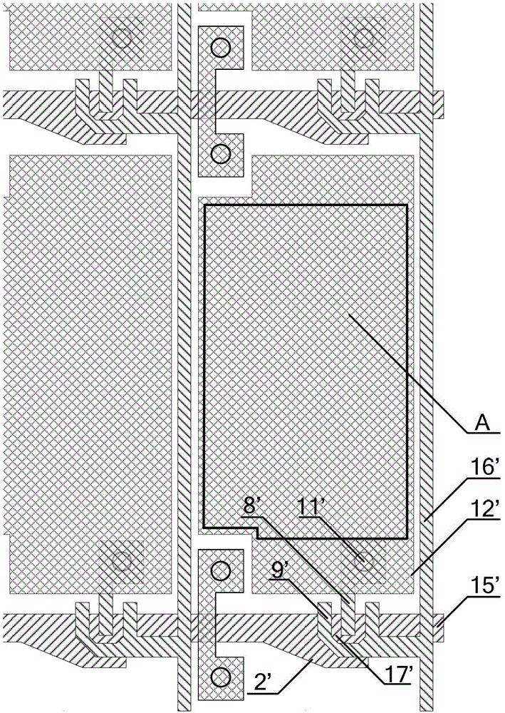
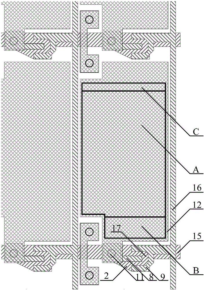
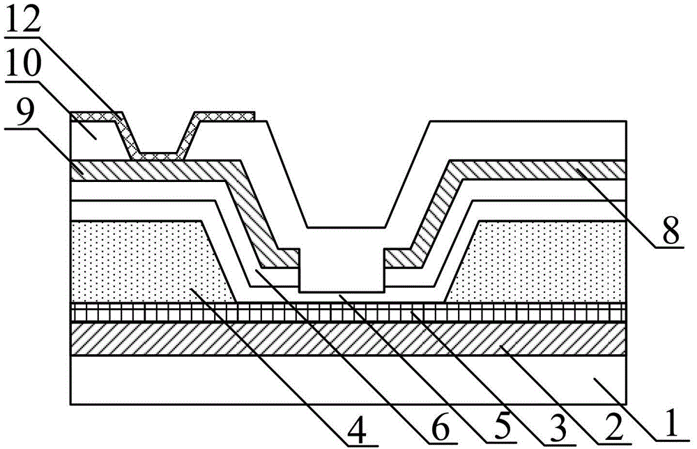
[0070] like figure 2 An array substrate shown in the figure, the structure of a pixel unit is shown in the figure; image 3 Yes figure 2 A cross-sectional view of the mid-array substrate; it includes data lines 16 and gate lines 15 formed on the substrate 1, the data lines 16 and the gate lines 15 define a pixel area, and a thin film transistor and a pixel electrode 12 are formed in the pixel area, and the gate lines 15 is used to provide a turn-on signal to the thin film transistor, and the data line 16 is used to provide a data signal to the pixel electrode 12; the thin film transistor includes: a gate electrode 2 formed on the substrate 1 and connected to the gate line 15; formed on the gate line 15 and the gate The gate insulating layer 3 on the electrode 2 and covering the entire substrate; the active layer formed on the gate insulating layer 3, the drain electrode 8 formed above the active layer and the source electrode opposite to the drain electrode 8 and connected ...

Embodiment 2

[0076] The present invention also provides a method for preparing the above-mentioned array substrate, which mainly includes forming gate lines and gate electrodes on the substrate, and forming a gate insulating layer covering the entire substrate on the gate lines and gate electrodes; Drain electrode and source electrode; a filling layer is formed between the gate electrode and the drain electrode and the source electrode; a passivation layer is formed on the source electrode, the drain electrode and the channel region; the position where the passivation layer is located above the gate line and the drain electrode Opening a passivation layer via hole; forming a pixel electrode connected to the drain electrode through the passivation layer via hole. In this embodiment, a filling layer is formed between the gate electrode, the drain electrode and the source electrode as an example for description.

[0077] Flow chart such as Figure 4 The shown method for preparing an array su...

Embodiment 3

[0101] The present invention also provides a display device including any one of the above array substrates.

[0102] The present invention also provides a display device, including the array substrate described in the first embodiment; because the pixel aperture ratio is increased, the display device has light transmittance and resolution, and because the energy consumption of the backlight module is reduced , saving costs and improving display quality.

[0103] The above-mentioned display device may be a display panel, electronic paper, OLED (Organic Light Emitting Diode, organic light-emitting diode) panel, liquid crystal TV, liquid crystal display, digital photo frame, mobile phone, tablet computer and other products or components with any display function.


PUM


Abstract

An array substrate, a manufacturing method thereof and a display device are provided, and the array substrate comprises: a substrate (1); a plurality of data lines (16), formed on the substrate and extending in a first direction; a plurality of gate lines (15), formed on the substrate (1), crossing the plurality of data lines (15), and extending in a second direction perpendicular to the first direction; a plurality of pixel regions, defined by the plurality of gate lines (15) and the plurality of data lines (15) crossing each other and arranged in a matrix form, wherein each of the pixel regions is provided with a thin film transistor and a pixel electrode (12), wherein, the thin film transistor comprises: a gate electrode (2), connected with one of the plurality of gate lines (15); a gate insulating layer (3), provided above the gate line (15) and the gate electrode (2); an active layer (5), formed on the gate insulating layer (3) and disposed corresponding to the gate electrode (2); a drain electrode (8) and a source electrode (9), disposed opposite to each other above the active layer (5) and having a channel region of the thin film transistor therebetween; a filling layer (4), provided between the gate electrode (2) and the gate line (15) connected with the gate electrode, and the drain and source electrodes (8) and (9); and a passivation layer (10), provided on the source electrode (9), the drain electrode (8) and the active layer (5), wherein at a position directly facing the gate line (15), the passivation layer (10) is provided with a passivation layer through hole (11) configured to perform a connection between the drain electrode (8) and the pixel electrode (12).

Description

technical field [0001] The invention relates to the technical field of liquid crystal display, in particular to an array substrate, a method for preparing the array substrate and a display device. Background technique [0002] Liquid Crystal Display (LCD) has now occupied the dominant position in the field of flat panel display due to its advantages of stable picture, vivid image, radiation elimination, space saving and energy saving. TFT-LCD (Thin Film Transistor-Liquid Crystal Display, thin film transistor liquid crystal display) is the current mainstream liquid crystal display. [0003] A very important specification in a liquid crystal display is the light transmittance, and the most important factor determining the light transmittance is the aperture ratio. The aperture ratio is simply the ratio of the effective area through which light can pass; the liquid crystal panel includes an array substrate and a color filter substrate. The schematic diagram of the array substr...

Claims


Application Information

Patent Timeline
Patent Type & Authority Patents(China)
IPC IPC(8): H01L29/786H01L27/12H01L21/77G02F1/1362G02F1/1368
CPCG02F1/1368H01L23/3171H01L21/76802H01L27/1259H01L29/4175H01L27/124H01L29/66765H01L29/78696H01L21/283G02F2201/40G02F1/1362H01L27/1248H01L27/1288H01L29/41733G02F1/136227H01L29/1033H01L21/32133H01L2924/0002H01L2924/00
Inventor 金熙哲宋泳锡刘圣烈崔承镇
Owner BOE TECH GRP CO LTD
Why Eureka
Try Eureka