Wafer Fragmentation Method and Its Application

A wafer and wafer technology, applied in the wafer splitting method and its application field, can solve the problems of long sample preparation time, expensive equipment, complicated equipment, etc., to simplify the splitting process, increase accuracy and stability, and shorten the splitting time Effect

Active Publication Date: 2020-12-11
南京晶驱集成电路有限公司
View PDF3 Cites 0 Cited by
  • Summary
  • Abstract
  • Description
  • Claims
  • Application Information

AI Technical Summary

Problems solved by technology

The disadvantage of this method is that the equipment is complicated, and it needs to be equipped with complex structures...

Method used


Image

  • Wafer Fragmentation Method and Its Application
  • Wafer Fragmentation Method and Its Application
  • Wafer Fragmentation Method and Its Application

Examples


Embodiment Construction

[0042] In order to make the purpose, advantages and features of the present invention clearer, the wafer splitting method and the wafer failure analysis method proposed by the present invention will be further described in detail below. It should be noted that, the accompanying drawings are all in a very simplified form and in inaccurate scales, and are only used to facilitate and clearly assist the purpose of explaining the embodiments of the present invention.

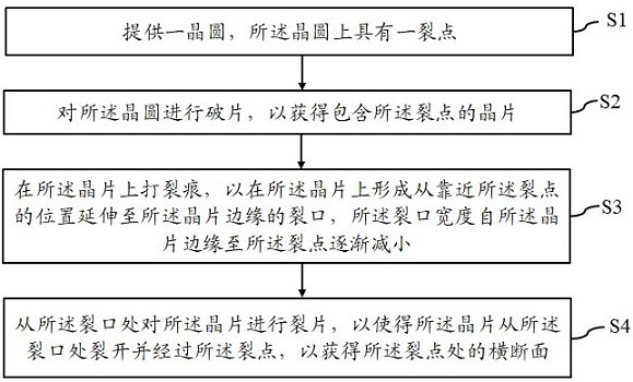
[0043] An embodiment of the present invention provides a wafer splitting method, refer to image 3 , image 3 It is a flowchart of a wafer splitting method according to an embodiment of the present invention, and the wafer splitting method includes:

[0044] Step S1, providing a wafer with a crack on the wafer;

[0045] Step S2, fragmenting the wafer to obtain a wafer containing the crack;

[0046] Step S3, making a crack on the wafer to form a crack on the wafer extending from a position close to the crack point ...


PUM


Abstract

The present invention provides a method for splitting a wafer and its application. The method for splitting a wafer includes: providing a wafer with a split point on the wafer; splitting the wafer to obtain the A cracked wafer; a crack is made on the wafer to form a crack extending from a position close to the crack point to the edge of the wafer on the wafer, and the crack width is from the edge of the wafer to the crack the point tapers; and splitting the wafer from the break such that the wafer is split from the break and past the break point to obtain a cross-section at the break point. The technical scheme of the invention enables the splitting process to be simplified to shorten the splitting time, and at the same time, the splitting precision can reach micron level, thereby enabling rapid and effective failure analysis on the wafer.

Description

technical field [0001] The invention relates to the field of integrated circuit manufacturing, in particular to a wafer splitting method and application thereof. Background technique [0002] In the process of semiconductor process development or the process of semiconductor device manufacturing failure analysis, it is a very common method to analyze the cross-sectional topography of a specific pattern on a wafer. The basic steps include: first, the wafer (including The silicon substrate and the film layers and patterns on the silicon substrate) are cracked along the pattern to be observed to obtain a cross-section of the pattern, such as figure 1 As shown, the wafer was cleaved along the AA' section to obtain the topography of the cross section here, as figure 2 As shown, the internal topography of the gate electrode 11, the source electrode 12 and the drain electrode 13 formed on the substrate 10 can be obtained; Zoom in to view a cross-section of the graph. [0003] A...

Claims


Application Information

Patent Timeline
IPC IPC(8): H01L21/78H01L21/66
CPCH01L21/78H01L22/30
Inventor 陈曦
Owner 南京晶驱集成电路有限公司
Why Eureka
Try Eureka