Preparation method of heterostructure thin film capable of reducing thin film stripping thermal stress

A heterogeneous structure, film stripping technology, applied in the manufacture/assembly of piezoelectric/electrostrictive devices, electrical components, piezoelectric/electrostrictive/magnetostrictive devices, etc., can solve the problem of poor quality, piezoelectric thin films Fragmentation, large thermal stress, etc.

Active Publication Date: 2020-10-20
SHANGHAI NOVEL SI INTEGRATION TECH CO LTD
View PDF8 Cites 3 Cited by
  • Summary
  • Abstract
  • Description
  • Claims
  • Application Information

AI Technical Summary

Problems solved by technology

[0004] What the present invention aims to solve is that the thermal stress in the preparation process of the piezoelectric film is large, so that in the process of peeling and transferring the film, it is easy to cause the technical problem of splitting and poor quality of the piezoelectric film

Method used


Image

  • Preparation method of heterostructure thin film capable of reducing thin film stripping thermal stress
  • Preparation method of heterostructure thin film capable of reducing thin film stripping thermal stress
  • Preparation method of heterostructure thin film capable of reducing thin film stripping thermal stress

Examples


Embodiment Construction

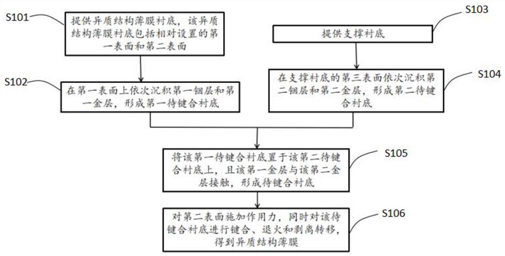
[0042] The technical solutions in the embodiments of the present application will be clearly and completely described below in conjunction with the drawings in the embodiments of the present application. Apparently, the described embodiments are only some of the embodiments of this application, not all of them. Based on the embodiments in this application, all other embodiments obtained by persons of ordinary skill in the art without creative efforts fall within the protection scope of this application.

[0043] Reference herein to "one embodiment" or "an embodiment" refers to a specific feature, structure or characteristic that may be included in at least one implementation of the present application. In the description of the present application, it should be understood that the orientation or positional relationship indicated by the terms "upper", "lower", "top", "bottom" etc. is based on the orientation or positional relationship shown in the drawings, and is only for It ...


PUM

PropertyMeasurementUnit
thicknessaaaaaaaaaa
thicknessaaaaaaaaaa
melting pointaaaaaaaaaa

Abstract

The invention relates to the field of preparation of semiconductor materials, and discloses a preparation method of a heterostructure thin film capable of reducing thin film stripping thermal stress.The method specifically comprises the following steps: firstly, providing a heterostructure thin film substrate which comprises a first surface and a second surface which are oppositely arranged; sequentially depositing a first indium layer and a first gold layer on the first surface to form a first substrate to be bonded; secondly, providing a support substrate; sequentially depositing a second indium layer and a second gold layer on the third surface of the support substrate to form a second substrate to be bonded; placing a first to-be-bonded substrate on a second to-be-bonded substrate, and enabling the first gold layer to be in contact with the second gold layer to form a to-be-bonded substrate; and finally, applying an acting force to the second surface, and meanwhile, carrying out bonding, annealing and stripping transfer on the substrate to be bonded to obtain the heterostructure film. The preparation method of the heterostructure film provided by the invention has the characteristics that the area of the peeled and transferred piezoelectric film is increased, and the film is not easy to crack.

Description

technical field [0001] The invention relates to the field of semiconductor material preparation, in particular to a preparation method of a heterogeneous structure thin film which reduces the peeling thermal stress of the thin film. Background technique [0002] In the preparation process of semiconductor devices, since the lift-off technology can avoid the problems of lattice mismatch and crystal form mismatch in the heteroepitaxial growth process, so as to realize the heterogeneous integration between mismatched materials, the lift-off technology is widely used Realize the heterogeneous integration of thin film materials. [0003] The commonly used piezoelectric material peeling method is to directly transfer the piezoelectric material film to the substrate, that is, the method of direct bonding. Generally, the thermal expansion coefficient of the piezoelectric material is quite different from that of the substrate material, so that In the subsequent peeling annealing, a ...

Claims


Application Information

Patent Timeline
Patent Type & Authority Applications(China)
IPC IPC(8): H01L41/313H01L41/33H01L41/22
CPCH10N30/01H10N30/073H10N30/08
Inventor 欧欣林家杰游天桂沈正皓金婷婷
Owner SHANGHAI NOVEL SI INTEGRATION TECH CO LTD
Why Eureka
Try Eureka