
bga heat dissipation structure and bga heat dissipation packaging method

A technology of heat dissipation structure and packaging method, which is applied in the direction of semiconductor/solid-state device parts, semiconductor devices, electrical components, etc. It can solve the problems of chip structure influence, product heat dissipation performance, chip and heat dissipation cover cavity, etc., to ensure heat dissipation performance effect

Active Publication Date: 2020-12-15
FOREHOPE ELECTRONICS NINGBO CO LTD
View PDF3 Cites 0 Cited by
  • Summary
  • Abstract
  • Description
  • Claims
  • Application Information

AI Technical Summary

Problems solved by technology

Due to the volatility of the flux and the low melting point of heat sinks such as indium, the flux continuously releases gas during the reflow process, and the volatilized gas of the flux will displace the melted heat sink, causing the formed mixture to overflow to the bottom The chip will affect the structure of the chip. At the same time, the mixture overflows too much, which will cause a large number of voids between the chip and the heat dissipation cover, which will affect the heat dissipation performance of the product.

Method used


Image

  • bga heat dissipation structure and bga heat dissipation packaging method
  • bga heat dissipation structure and bga heat dissipation packaging method
  • bga heat dissipation structure and bga heat dissipation packaging method

Examples


no. 1 example

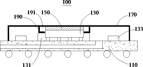
[0049] Please refer to figure 1 , this embodiment provides a BGA heat dissipation structure 100, which can prevent the overflowing mixture from affecting the structural safety of the chip 130 during reflow soldering, and can prevent too much overflowing of the mixture from affecting the heat dissipation performance, and at the same time can make the glue be heated more uniformly. Avoid product damage.

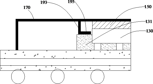
[0050]The BGA heat dissipation structure 100 provided in this embodiment includes a substrate 110, a chip 130, a heat sink 150 and a heat dissipation cover 170. The chip 130 is mounted on the substrate 110, the heat sink 150 is mounted on the chip 130, and the heat dissipation cover 170 is covered on the On the substrate 110 around the chip 130, and mounted on the heat sink 150, wherein, the heat dissipation cover 170 is provided with an overflow ring structure 190, the overflow ring structure 190 is arranged around the chip 130, and forms an overflow groove 191, and the overfl...

no. 2 example

[0070] This embodiment provides a BGA heat dissipation structure 100. Its basic structure, principle and technical effect are the same as those of the first embodiment. For a brief description, the part not mentioned in this embodiment can refer to the Correspondingly, the difference between this embodiment and the first embodiment lies in the structure of the substrate 110 .

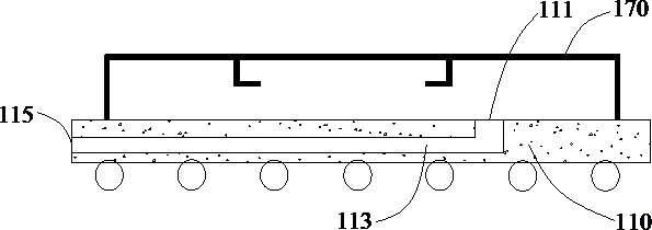
[0071] see Figure 4 , in this embodiment, the bottom of the heat dissipation cover 170 is bonded to the substrate 110 by a sealant to form an internal cavity. The upper surface of the substrate 110 is also provided with an internal exhaust hole 111 communicating with the internal cavity. The substrate 110 is also provided with an exhaust groove 113 communicating with the internal exhaust hole 111. The exhaust groove 113 is arranged below the chip 130 and extends to the external space. The bottom surface of the substrate 110 is also provided with a bottom exhaust hole 117. The bottom exhaust hole 117 c...

no. 3 example

[0076] This embodiment provides a BGA heat dissipation structure 100. Its basic structure, principle and technical effect are the same as those of the first embodiment. For a brief description, the part not mentioned in this embodiment can refer to the Correspondingly, the difference between this embodiment and the first embodiment lies in the structure of the substrate 110 .

[0077] see Figure 5, in this embodiment, the bottom of the heat dissipation cover 170 is bonded to the substrate 110 by a sealant to form an internal cavity. The upper surface of the substrate 110 is also provided with an internal exhaust hole 111 communicating with the internal cavity. The substrate An exhaust groove 113 communicating with the internal exhaust hole 111 is also provided in the 110, and the exhaust groove 113 is arranged under the chip 130 and extends to the external space.

[0078] In this embodiment, a side wall exhaust hole 115 is further provided on the side wall of the substrate 1...


PUM


Abstract

The embodiment of the invention provides a BGA heat dissipation structure and a BGA heat dissipation packaging method, relating to the technical field of chip packaging. The BGA heat dissipation structure comprises a substrate, a chip, a cooling fin and a cooling cover, wherein the chip is attached to the substrate, the cooling fin is attached to the chip, the cooling cover covers the substrate around the chip and is attached to the cooling fin, an overflow ring structure is arranged on the cooling cover, the overflow ring structure is arranged around the chip in a surrounding mode and forms an overflow groove, and the distance between the overflow groove and the substrate is smaller than the distance between the cooling fin and the substrate. According to the invention, the containing space is formed through the overflow groove to contain the mixture formed by the gas generated by the soldering flux of the cooling fin and the molten cooling fin, so that the mixture is prevented from falling to the lower part of the chip to influence the structural safety of the chip, and meanwhile, a large number of holes caused by insufficient materials of the cooling fin due to excessive fallingof the mixture are avoided, thereby ensuring the heat dissipation performance.

Description

technical field [0001] The invention relates to the technical field of chip packaging, in particular to a BGA heat dissipation structure and a BGA heat dissipation packaging method. Background technique [0002] With the rapid development of the semiconductor industry, the BGA ball grid array package (Ball Grid Array Package) packaging structure is widely used in the semiconductor industry. Generally, the BGA packaging structure is used to achieve heat dissipation by mounting the heat dissipation cover. The heat dissipation cover is required to meet the heat dissipation. The chip usually adopts flip chip technology. Due to the volatility of the flux and the low melting point of heat sinks such as indium, the flux continuously releases gas during the reflow process, and the volatilized gas of the flux will displace the melted heat sink, causing the formed mixture to overflow to the bottom The chip will affect the structure of the chip, and the mixture will overflow too much,...

Claims


Application Information

Patent Timeline
Patent Type & Authority Patents(China)
IPC IPC(8): H01L23/367H01L23/04H01L21/52
CPCH01L21/52H01L23/04H01L23/367H01L2224/73253
Inventor 何正鸿庞宏林
Owner FOREHOPE ELECTRONICS NINGBO CO LTD
Learn More