Pixel arrangement structure and display panel

A technology of pixel arrangement and array structure, applied in electrical components, electrical solid-state devices, circuits, etc., can solve the problems of reducing the ink deposition area, reducing the light-emitting area, and affecting the resolution of the display panel.

Active Publication Date: 2020-11-03
GUANGDONG JUHUA PRINTING DISPLAY TECH CO LTD
View PDF6 Cites 4 Cited by
  • Summary
  • Abstract
  • Description
  • Claims
  • Application Information

AI Technical Summary

Problems solved by technology

[0004] However, in the field of printing technology, in order to improve the light transmittance of the entire transparent display panel, it is often necessary to sacrifice part of the light-emitting area as the light-transmitting area, which leads to the reduction of the ink deposition area and the reduction of the light-emitting area, which in turn affects the resolution of the display panel. Therefore, printing technology has great challenges in obtaining high-resolution transparent display panels

Method used


Image

  • Pixel arrangement structure and display panel
  • Pixel arrangement structure and display panel
  • Pixel arrangement structure and display panel

Examples


preparation example Construction

[0061] A method for preparing a display panel according to another embodiment of the present invention includes the following steps:

[0062] S101: Provide a substrate.

[0063] The driving circuit array can be fabricated on the substrate through the yellow light process.

[0064] S102: Fabricate patterned pixel electrodes in each light emitting region of the substrate.

[0065] A planarization layer may also be formed in the light emitting region of the substrate where the pixel electrode is formed. By forming a flat layer, the uneven surface caused by the driving circuit can be covered, which is beneficial to the formation of subsequent layers. The planar layer can be made of organic materials and prepared by inkjet printing, which is not particularly limited here.

[0066] S103: Fabricate a pixel defining layer in the light-emitting region of the substrate, and define several pixel pits to form a light-emitting region and a light-transmitting region corresponding to the ...

Embodiment 1

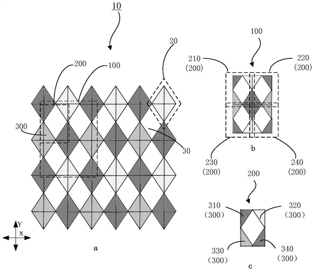
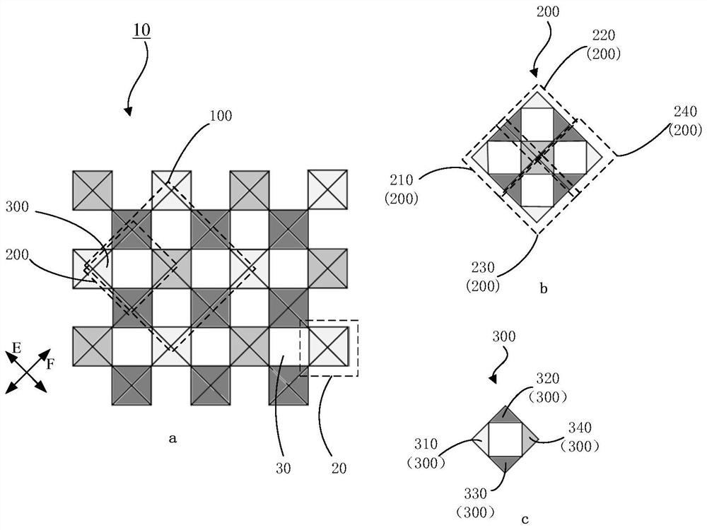
[0075] Such as figure 1 As shown, the pixel arrangement structure 10 of this embodiment includes a plurality of repeating units 100, and the repeating units 100 are arranged along the row direction and the column direction ( figure 1 In the X direction and the Y direction, X and Y are perpendicular to each other), forming an array structure; the repeating unit 100 is divided into four pixel units 200 of 2×2 along the row direction and the column direction, which are respectively the first pixel unit 210 and the second pixel unit 210 unit 220, the third pixel unit 230 and the fourth pixel unit 240, the first pixel unit 210 and the fourth pixel unit 240 are centrally symmetrical, the second pixel unit 220 and the third pixel unit 230 are centrally symmetrical, and the first pixel unit 210 . The center of symmetry of the fourth pixel unit 240 coincides with the centers of symmetry of the second pixel unit 220 and the third pixel unit 230 .

[0076] Each pixel unit 200 includes f...

Embodiment 2

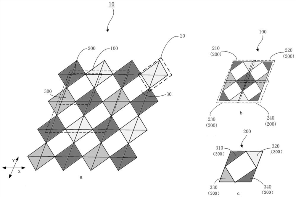
[0079] Such as figure 2 As shown, the pixel arrangement structure 10 of this embodiment includes a plurality of repeating units 100, and the repeating units 100 are arranged along the row direction and the column direction ( figure 1 In the X direction and Y direction, X and Y have a certain angle), forming an array structure; the repeating unit 100 is divided into four pixel units 200 of 2×2 along the row direction and the column direction, which are the first pixel unit 210, the second pixel unit 200, respectively. The second pixel unit 220, the third pixel unit 230 and the fourth pixel unit 240, the first pixel unit 210 and the fourth pixel unit 240 are centrally symmetrical, the second pixel unit 220 and the third pixel unit 230 are centrally symmetrical, and the first The symmetry centers of the pixel unit 210 and the fourth pixel unit 240 coincide with the symmetry centers of the second pixel unit 220 and the third pixel unit 230 .

[0080] Each pixel unit 200 includes...


PUM


Abstract

The invention relates to a pixel arrangement structure and a display panel, the pixel arrangement structure comprises a plurality of polygonal repetitive units, each repetitive unit comprises 2n pixelunits arranged around the central point of the repetitive unit, wherein n is an integer greater than or equal to 2; each pixel unit comprises a plurality of sub-pixels, the plurality of sub-pixels have at least three light-emitting colors, and the light-emitting colors of the adjacent sub-pixels are different; a light-transmitting area is arranged in each pixel unit, and all sub-pixels in each pixel unit are arranged around the corresponding light-transmitting area. In the pixel arrangement structure, the adjacent repeating units are arranged in an edge-to-edge mode, so that the sub-pixels which are located at the adjacent positions in the repeating units and have the same light-emitting color are gathered together, and a light-emitting area in a regular shape is formed. According to thepixel arrangement structure, the resolution of the display panel can be improved on the premise that the preparation difficulty is not improved.

Description

technical field [0001] The invention relates to the technical field of electronic display, in particular to a pixel arrangement structure and a display panel. Background technique [0002] As a new display technology, transparent display allows observers to see the background behind the display screen through the display screen. This display technology expands the application field of traditional display technology and can be used in mobile phones, computers, refrigerators, display , billboards and other fields. [0003] Organic light-emitting diodes (OLEDs) and quantum dot light-emitting diodes (QLEDs) are currently important directions for the development of transparent display panels due to their light and thin characteristics. This type of display panel is mainly produced by solution processing, especially printing technology, which is considered to be the most effective way to realize OLED and QLED low-cost and large-area full-color display. [0004] However, in the f...

Claims


Application Information

Patent Timeline
Patent Type & Authority Applications(China)
IPC IPC(8): H01L27/32
CPCH10K59/353
Inventor 史文陈亚文
Owner GUANGDONG JUHUA PRINTING DISPLAY TECH CO LTD
Why Eureka
Try Eureka