A latch-type amplifier offset elimination method and offset elimination circuit

A technology for eliminating circuits and amplifiers. It is applied in the direction of improving amplifiers to improve efficiency and improving amplifiers to reduce noise effects. It can solve problems such as limited application range, charge loss, and limited actual effect, and achieves improved application range, improved amplification accuracy, The effect of eliminating dissonance

Active Publication Date: 2022-08-05
HUBEI UNIV
View PDF4 Cites 0 Cited by
  • Summary
  • Abstract
  • Description
  • Claims
  • Application Information

AI Technical Summary

Problems solved by technology

attached figure 2 The source is paper 1: [LatchOffset Cancellation Sense Amplifier for Deep Submicrometer STT-RAM, IEEETRANSACTIONS ON CIRCUITS AND SYSTEMS—I: REGULAR PAPERS, VOL.62, NO.7, JULY 2015:1776-1784], by which figure 2 It can be seen that the circuit does not use capacitors for offset storage, but in the P2 phase, by applying the reference voltage VREF to the gate of M1, the gate and drain of M2, it can store the offset caused by the mismatch between M1 and M2 offset voltage, as attached image 3 As shown, this structure can only eliminate the offset voltage caused by the mismatch between M1 and M2, but cannot eliminate the offset voltage introduced by M3 and M4 when performing positive feedback amplification in the P4 stage
In addition, this structure also requires that the input signal must be able to provide driving capability for a long time. In the P1, P2 and P3 stages, the input needs to be connected to the circuit, and there is a charge loss. Therefore, it is only suitable for resistive input and cannot be used for capacitive input. In the case of sexual input
[0004] attached Figure 4 The source is paper 2: [A 45nm Self-Aligned-Contact Process 1Gb NOR Flashwith 5MB / s Program Speed, ISSCC 2008, SESSION 23, NON-VOLATILE MEMORY, 23.3:423-424], the circuit introduces two offset memory Capacitor, in the P2 stage, the offset caused by the mismatch of the two NMOS input pair tubes is eliminated. Although this structure is suitable for capacitive input, it cannot eliminate the offset caused by the PMOS input pair tube mismatch, and the actual effect is limited.
[0005] Synthesizing the status quo of offset cancellation of latch-type sampling amplifiers, it can be concluded that the existing offset cancellation methods generally have the following shortcomings: they cannot simultaneously cancel the offset of all input transistors, and cannot be applied to both resistive and capacitive input conditions, so that the latch-type amplifier cannot be applied to tiny signal amplification applications, which greatly limits its application range

Method used


Image

  • A latch-type amplifier offset elimination method and offset elimination circuit
  • A latch-type amplifier offset elimination method and offset elimination circuit
  • A latch-type amplifier offset elimination method and offset elimination circuit

Examples


Embodiment

[0039] Implementation example: Figure 5 Shown is an implementation example of a latch-type amplifier offset cancellation circuit of the present invention. Input A and output B of the first inverter INV1 are connected to one end of C0 and C1 respectively, and input C and output D of the second inverter INV2 are connected to one end of C3 and C2 respectively. The specific circuit includes:

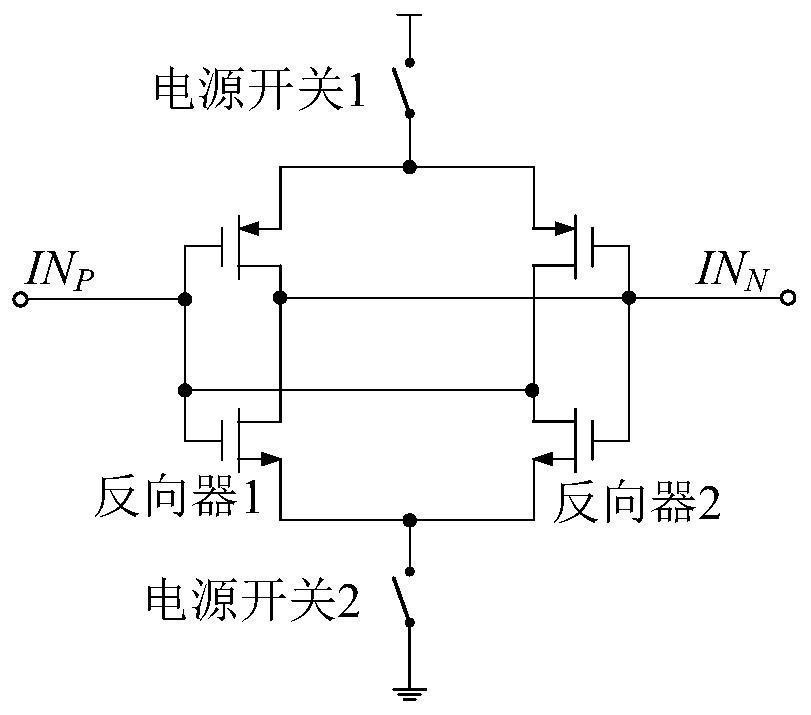
[0040] The first inverter INV1 and the second inverter INV2, four capacitors C0-C3, and twelve switches S1-S12, further include: a third inverter INV3 and a fourth inverter INV4; the first inverter INV3 and the fourth inverter INV4; The inverter INV1 and the second inverter INV2 are both amplifying inverters, the third inverter INV3 and the fourth inverter INV4 are two shaping inverters; the first inverter INV1 includes: a first transistor PMOS1 and the second transistor NMOS1, the gates of the input terminals of the first transistor PMOS1 and the second transistor NMOS1 are connected in ...


PUM


Abstract

The invention discloses an offset elimination method and an offset elimination circuit of a latch type amplifier. The circuit includes two inverters for amplifying, four capacitors, 12 switches and two inverters for shaping. The input and output terminals of each amplifying inverter are respectively connected with each capacitor, and each switch is respectively connected between each inverter and the common mode level, power supply, ground, input and output signals; The discharged four capacitors store the mismatch between the four input tubes of the latch-type amplifier, and then perform sampling, pre-amplification and positive feedback rail-to-rail amplification of the input signal respectively, which can adjust all the input transistors of the latch-type amplifier. The offset caused by the mismatch is effectively eliminated, and it is suitable for both resistive and capacitive input conditions, which greatly improves its amplification accuracy, so that it has a similar offset suppression performance as an analog amplifier and expands its scope of application.

Description

technical field [0001] The invention relates to an offset elimination method and an offset elimination circuit of a latch type amplifier, in particular to an offset voltage that can eliminate the offset voltage caused by the mismatch of all input transistors of a latch type amplifier, and is suitable for resistive and capacitive input conditions at the same time. An offset elimination method and an offset elimination circuit for realizing the offset elimination method belong to the technical field of integrated circuit design. Background technique [0002] In the CMOS process, latch-type amplifiers can directly output rail-to-rail amplified signals due to their simple structure, and are widely used. as attached figure 1 As shown, the latch-type amplifier is usually composed of two inverters connected end to end and two power switches. When sampling and amplifying an external signal, first the two power switches are turned off, and the two inverters are connected to the powe...

Claims


Application Information

Patent Timeline
Patent Type & Authority Patents(China)
IPC IPC(8): H03F1/02H03F1/26
CPCH03F1/02H03F1/26
Inventor 万美琳鲍磊张寅贺章擎彭旷胡永明顾豪爽
Owner HUBEI UNIV
Why Eureka
Try Eureka