Eureka AIR delivers breakthrough ideas for toughest innovation challenges, trusted by R&D personnel around the world.

Display device and manufacturing method thereof

A technology for display devices and scattering particles, which is used in the manufacture of semiconductor/solid-state devices, electric solid-state devices, semiconductor devices, etc. problem, to achieve the effect of improving the light extraction efficiency and improving the low light conversion efficiency

Inactive Publication Date: 2020-11-06
SHENZHEN CHINA STAR OPTOELECTRONICS SEMICON DISPLAY TECH CO LTD
View PDF2 Cites 6 Cited by
  • Summary
  • Abstract
  • Description
  • Claims
  • Application Information

AI Technical Summary

Problems solved by technology

[0003] However, when perovskite luminescent materials are used as the color conversion layer, there are factors such as poor light absorption and light extraction rate, resulting in low light conversion efficiency of the color conversion layer.
Low light conversion efficiency directly affects the energy utilization and brightness of display devices, which is not conducive to the further development of high-performance display devices

Method used


Image

  • Display device and manufacturing method thereof
  • Display device and manufacturing method thereof
  • Display device and manufacturing method thereof

Examples


Embodiment Construction

[0032] In order to make the purpose, technical solution and advantages of the present invention clearer, the present invention will be further described in detail below in conjunction with the accompanying drawings, please refer to the drawings in the accompanying drawings, wherein the same component symbols represent the same components, the following description is Based on the particular embodiment of the invention shown, it should not be construed as limiting the invention to other embodiments not detailed herein. The word "embodiment" as used in this specification means an example, instance or illustration.

[0033] In the description of the present application, it should be understood that the terms "center", "longitudinal", "transverse", "length", "width", "thickness", "upper", "lower", "front", " Orientation indicated by rear, left, right, vertical, horizontal, top, bottom, inside, outside, clockwise, counterclockwise, etc. The positional relationship is based on the ...


PUM


Abstract

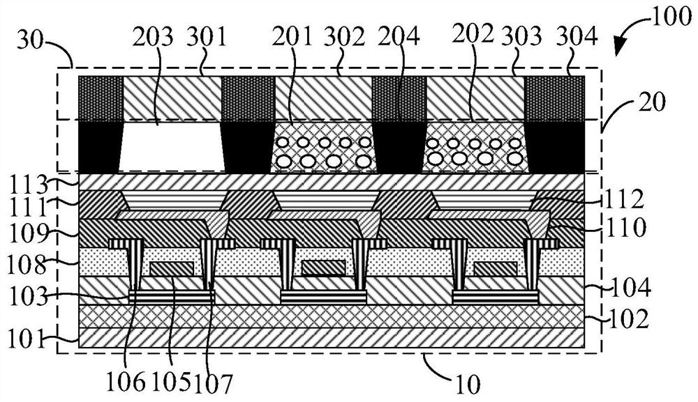
The invention discloses a display device and a manufacturing method thereof. The display device includes: a light-emitting back plate, a color conversion layer and a color film layer, the color conversion layer is arranged on the light-emitting back plate; the color conversion layer comprises a red light conversion unit, a green light conversion unit and an opening unit; wherein the red light conversion unit and / or the green light conversion unit comprise / comprises a perovskite light-emitting material and scattering particles arranged in the perovskite light-emitting material in a stacked mode, and the refractive index of the scattering particles is gradually increased in the vertical direction from the face, close to the light-emitting back plate, of the color conversion layer to the face, away from the light-emitting back plate, of the color conversion layer; the color film layer is arranged on the color conversion layer, the color film layer comprises a red color resistance block, ablue color resistance block and a green color resistance block, which are arranged at intervals, and the red color resistance block, the green color resistance block and the blue color resistance block are respectively arranged corresponding to the red light conversion unit, the green light conversion unit and the opening unit.

Description

technical field [0001] The invention relates to the field of display technology, in particular to a display device and a manufacturing method thereof. Background technique [0002] OLED (Organic Light Emitting Diode, organic light-emitting diode) display device, also known as organic electroluminescent display device, due to the simple preparation process, low cost, low power consumption, high luminous brightness, wide range of operating temperature, light and thin volume, responsive The speed is fast, and it is easy to realize color display and large-screen display, easy to realize matching with integrated circuit driver, and easy to realize flexible display, so it has broad application prospects. Pe-OLED (Perovskite Organic Light Emitting Diode, Perovskite Organic Light Emitting Diode) is a new type of self-emitting diode. Compared with OLED, Pe-OLED has the advantages of high color purity and low material cost. Compared with QD-OLED (Quantum Dot Organic Light Emitting Di...

Claims


Application Information

Patent Timeline
IPC IPC(8): H01L27/32H01L51/52H01L51/56
CPCH10K59/38H10K59/12H10K50/854H10K59/1201H10K71/00H10K59/877
Inventor 吴永伟
Owner SHENZHEN CHINA STAR OPTOELECTRONICS SEMICON DISPLAY TECH CO LTD
Why Eureka
Eureka Blog
Learn More