
Chip carrier and semiconductor packaging product comprising chip carrier

A chip carrier and semiconductor technology, applied in semiconductor devices, semiconductor/solid-state device parts, electric solid-state devices, etc., can solve problems such as easy heat generation, affecting chip performance, and limited heat dissipation performance of semiconductor packaging products, achieving high reliability , the effect of good heat dissipation performance

Pending Publication Date: 2020-11-13
GREAT TEAM BACKEND FOUNDRY (DONGGUAN) LTD
View PDF9 Cites 0 Cited by
  • Summary
  • Abstract
  • Description
  • Claims
  • Application Information

AI Technical Summary

Problems solved by technology

[0002] Semiconductors are used in integrated circuits, consumer electronics, communication systems, photovoltaic power generation, lighting, high-power power conversion and other fields; semiconductor packaging products are to fix the chip (or chip) to the corresponding chip carrier, between the chip and the chip carrier After completing the necessary electrical connections, in order to prevent the internal circuit from being polluted by liquid, dust and gas in the environment, a layer of protective encapsulant is coated on the chip and the chip carrier to form a semiconductor package product; however, for high-power For semiconductor packaging products, the internal power devices tend to generate heat during operation. If the heat cannot be transferred to the outside of the semiconductor packaging product in a timely and effective manner, the accumulated heat will greatly affect the performance of the chip, thereby affecting the reliability of the semiconductor packaging product.
[0003] In the prior art, the heat generated by the chip is generally conducted to the outside atmosphere through the encapsulation compound. However, the thermal conductivity of the encapsulation compound is not good, which leads to the poor heat dissipation performance of the existing semiconductor packaging products.
There are still some semiconductor packaging products on the market. The heat dissipation of semiconductor packaging products is realized by adding metal radiators (such as toothed radiators) on the semiconductor packaging products. However, due to the heat exchange efficiency between the radiator and the chip, the heat dissipation The heat exchange efficiency between the device and the atmosphere is relatively limited, resulting in limited heat dissipation performance of existing semiconductor packaging products

Method used


Image

  • Chip carrier and semiconductor packaging product comprising chip carrier
  • Chip carrier and semiconductor packaging product comprising chip carrier
  • Chip carrier and semiconductor packaging product comprising chip carrier

Examples


Embodiment Construction

[0025] In order to make the technical problems solved by the present invention, the technical solutions adopted and the technical effects achieved clearer, the technical solutions of the embodiments of the present invention will be further described in detail below in conjunction with the accompanying drawings. Obviously, the described embodiments are only the technical solutions of the present invention. Some, but not all, embodiments. Based on the embodiments of the present invention, all other embodiments obtained by those skilled in the art without creative efforts fall within the protection scope of the present invention.

[0026] In the description of the present invention, unless otherwise clearly stipulated and limited, the terms "connected" and "fixed" should be understood in a broad sense, for example, it can be fixed connection, detachable connection or integration; it can be mechanical connection , can also be an electrical connection; it can be a direct connection...


PUM


Abstract

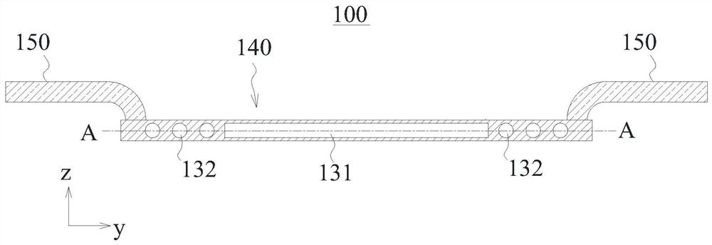
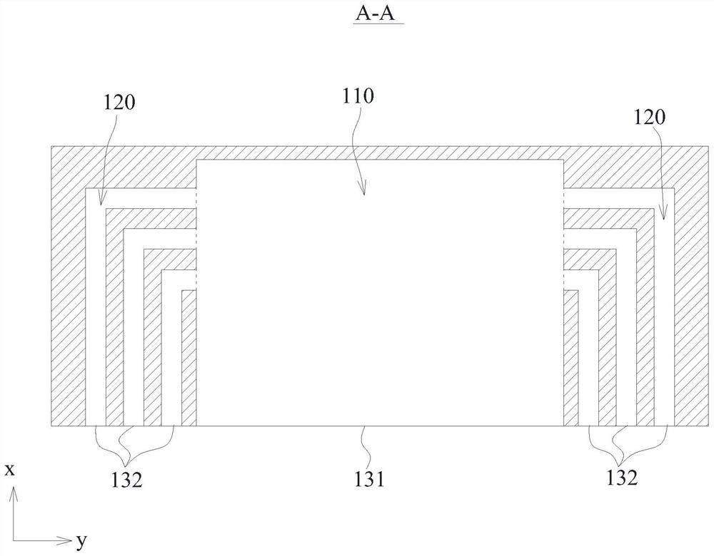
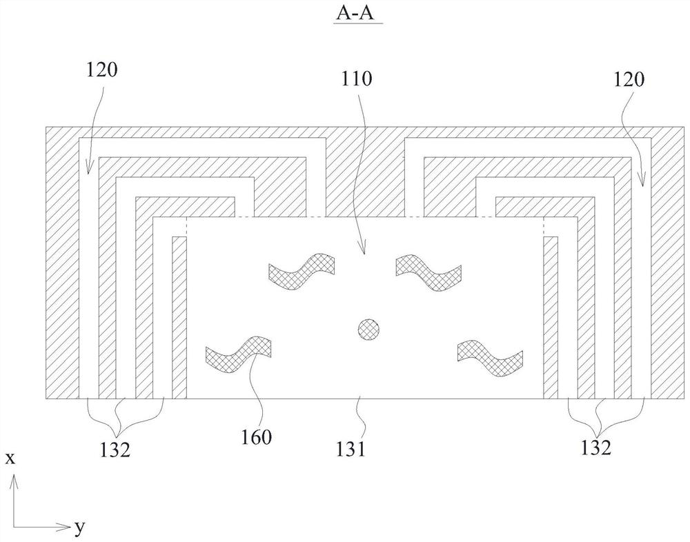
The invention discloses a chip carrier and a semiconductor packaging product comprising the chip carrier. The top of the chip carrier is used for bearing a chip. The chip carrier is provided with a liquid inlet cavity and is transversely provided with a plurality of lower heat dissipation channels; a lower liquid inlet and a plurality of lower liquid outlets are formed in the side wall of the chipcarrier; the liquid inlet cavity is communicated with the outside through the lower liquid inlet; one end of the lower heat dissipation channel is communicated with the liquid inlet cavity, and the other end of the lower heat dissipation channel is communicated with the outside through the lower liquid outlet; the semiconductor packaging product comprises the chip carrier and further comprises achip and packaging glue body, the chip is fixed to a chip carrying area of the chip carrier, and the packaging glue body wraps the chip and the chip carrier. The chip carrier and the semiconductor packaging product provided by the invention have good heat dissipation performance.

Description

technical field [0001] The invention relates to the technical field of semiconductor packaging, in particular to a chip carrier and a semiconductor packaging product. Background technique [0002] Semiconductors are used in integrated circuits, consumer electronics, communication systems, photovoltaic power generation, lighting, high-power power conversion and other fields; semiconductor packaging products are to fix the chip (or chip) to the corresponding chip carrier, between the chip and the chip carrier After completing the necessary electrical connections, in order to prevent the internal circuit from being polluted by liquid, dust and gas in the environment, a layer of protective encapsulant is coated on the chip and the chip carrier to form a semiconductor package product; however, for high-power For semiconductor packaging products, the internal power devices tend to generate heat during operation. If the heat cannot be transferred to the outside of the semiconductor...

Claims


Application Information

Patent Timeline
Patent Type & Authority Applications(China)
IPC IPC(8): H01L23/473H01L23/373H01L23/495
CPCH01L23/473H01L23/49568H01L23/3735H01L23/373H01L2224/48091H01L2924/181H01L2924/00014H01L2924/00012
Inventor 王琇如
Owner GREAT TEAM BACKEND FOUNDRY (DONGGUAN) LTD
Learn More