Backflow carrier

A carrier and bottom plate technology, applied in manufacturing tools, auxiliary devices, metal processing, etc., can solve the problems of false soldering of pins and unequal pin heights

Active Publication Date: 2020-11-17
华羿微电子股份有限公司
View PDF7 Cites 2 Cited by
  • Summary
  • Abstract
  • Description
  • Claims
  • Application Information

AI Technical Summary

Problems solved by technology

[0005] The embodiment of the present invention provides a reflow carrier, which is used to solve the problem of false soldering of the pins...

Method used


Image

  • Backflow carrier
  • Backflow carrier
  • Backflow carrier

Examples


Embodiment Construction

[0038] The following will clearly and completely describe the technical solutions in the embodiments of the present invention with reference to the accompanying drawings in the embodiments of the present invention. Obviously, the described embodiments are only some, not all, embodiments of the present invention. Based on the embodiments of the present invention, all other embodiments obtained by persons of ordinary skill in the art without making creative efforts belong to the protection scope of the present invention.

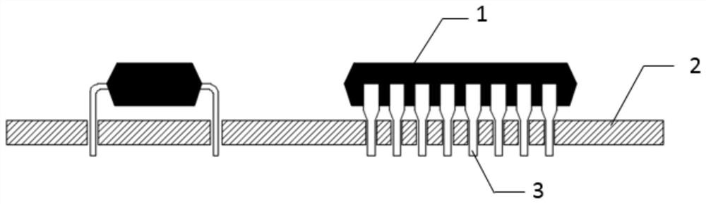
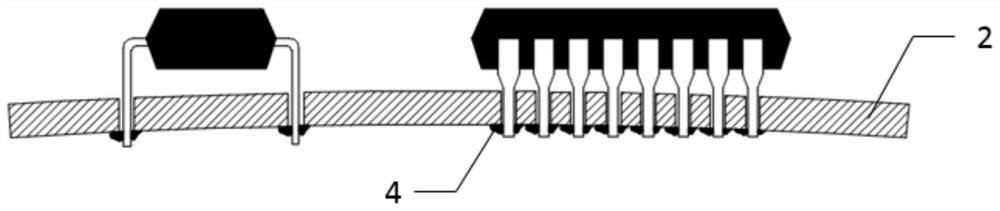
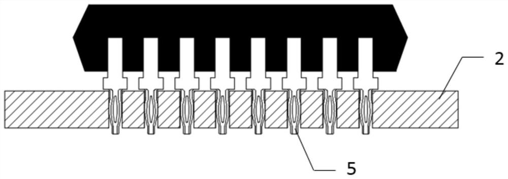
[0039] figure 1 It is a schematic diagram of welding and assembly of DIP products and PCB circuit boards in traditional technology; figure 2 It is a schematic diagram of the welding seam between the DIP product and the PCB circuit board in the traditional technology; image 3 It is a schematic diagram of the assembly of a DIP product with a medium-pressure fit pin and a PCB circuit board in the prior art; Figure 4 It is a schematic diagram of the connectio...


PUM


Abstract

The invention discloses a backflow carrier, and relates to the technical field of automobile-level intelligent power semiconductor module manufacturing. The problem that pins of a high-hardness lead frame are prone to cold solder joint due to uneven heights of the pins is solved. The backflow carrier comprises a backflow carrier bottom plate and a backflow carrier metal cover plate; the backflow carrier bottom plate comprises a substrate limiting groove, a frame limiting groove, a coarse positioning groove and a fine positioning pin; the substrate limiting groove is used for arranging a heat dissipation substrate, the frame limiting groove is used for arranging a high-hardness lead frame, and the coarse positioning groove and the fine positioning pin are used for arranging the backflow carrier metal cover plate; the backflow carrier metal cover plate comprises an operation handle, first protruding blocks and a first pressure connecting piece; the position of the operation handle corresponds to the position of the coarse positioning groove; the plurality of first protruding blocks are in contact with the upper surfaces of pin wires included in the high-hardness lead frame respectively; and the first pressure connecting piece is matched with a second pressure connecting piece arranged on the backflow carrier bottom plate to fix the backflow carrier metal cover plate to the backflow carrier bottom plate.

Description

technical field [0001] The invention relates to the technical field of automotive-grade intelligent power semiconductor module manufacturing, and more specifically relates to a reflow carrier. Background technique [0002] Power semiconductor module products that traditionally adopt DIP (English: dual in-line package, Chinese: dual in-line package) package shape design need to install the product to the PCB (English: Printed Circuit Board, Chinese: printed circuit board) by wave soldering. Circuit board) on the circuit board, wave soldering has high requirements on the flatness of the PCB circuit board, and it is easy to have bad problems such as missing soldering, bridging, and virtual soldering during the entire wave soldering process. At the same time, due to the high temperature in the soldering process , PCB circuit boards are also prone to warping, delamination and other undesirable phenomena. In order to solve the above problems, an intelligent power semiconductor mo...

Claims


Application Information

Patent Timeline
IPC IPC(8): B23K3/00B23K3/08
CPCB23K3/00B23K3/085B23K3/082
Inventor 蒋卫娟孙炎权郑阳斌
Owner 华羿微电子股份有限公司
Why Eureka
Try Eureka