
Patsnap Eureka
For R&D, Patsnap Eureka makes reading and utilizing patents & technical documents easy.
Patsnap Eureka AIR
Designed for self-driven R&D workflows. Generate viable solutions, solve complex R&D challenges, empower your innovation with AI.

Patsnap Eureka Materials
Designed for material experts only. Revolutionize your material R&D, from search, analyze, to developing new materials.

TechResearch
Generate reliable direction feasibility study reports for your R&D in just a few steps.

TechSeek
Discover and master advanced knowledge NOW. Basics, ideas, possibilities, all at once.

TechMind
As an expert in R&D Theories, TechMind can generates customized viable solutions instantly.

TechRisk
Analyze your overall solution with one click, know your potential R&D risks in advance.

TechMonitor
Get weekly tech updates, stay abreast of the latest tech innovations and key insights.
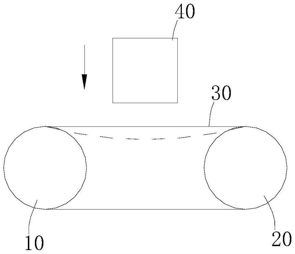
M12 large-size silicon wafer cutting method
A silicon wafer cutting, large-size technology, used in manufacturing tools, stone processing equipment, fine working devices, etc., can solve the problem of not being able to meet the requirements of M12 large-size wafer cutting
- Summary
- Abstract
- Description
- Claims
- Application Information
AI Technical Summary
Problems solved by technology
Method used
Image

Examples
Embodiment 1
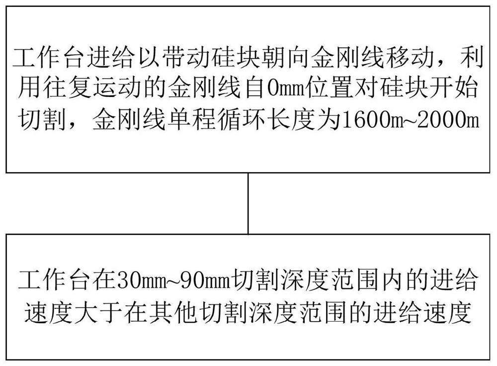
[0048] The diamond wire reciprocates, the one-way cycle length is 1600m, and the diamond wire speed is 35m / s. The initial feed speed of the table is 1mm / min; the feed speed of the table within the range of 0mm~30mm cutting depth is 1.2mm / min; the feed speed of the table within the range of 30mm~90mm cutting depth is 2.9mm / min; 90mm The feed speed of the table within the range of 180mm cutting depth is 2.7mm / min; the feed speed of the table within the range of 180mm~218mm cutting depth is 0.1~2.3mm / min. The cutting fluid temperature is 19°C. Cutting under the above parameter conditions, there is basically no disconnection. In addition, the TTV value of the silicon wafer is ≤25um, which meets the index requirements of the TTV value ≤30um.
Embodiment 2
[0050] The diamond wire reciprocates, the one-way cycle length is 1850m, and the diamond wire speed is 38m / s. The initial feed speed of the table is 1mm / min; the feed speed of the table within the range of 0mm~30mm cutting depth is 1.8mm / min; the feed speed of the table within the range of 30mm~90mm cutting depth is 2.95mm / min; 90mm The feed speed of the table within the range of ~180mm cutting depth is 2.62mm / min; the feed speed of the table within the range of 180mm~2180mm cutting depth is 0.1~2.2mm / min. The cutting fluid temperature is 20°C. Cutting under the above parameter conditions, there is basically no disconnection. In addition, the TTV value of the silicon wafer is ≤27um, which meets the index requirements of the TTV value ≤30um.
Embodiment 3
[0052] The diamond wire reciprocates, the one-way cycle length is 2000m, and the diamond wire speed is 40m / s. The initial feed speed of the table is 1mm / min; the feed speed of the table within the range of 0mm~30mm cutting depth is 2.2mm / min; the feed speed of the table within the range of 30mm~90mm cutting depth is 3mm / min; The feed speed of the table within the range of 180mm cutting depth is 2.7mm / min; the feed speed of the table within the range of 180mm~218mm cutting depth is 0.1~2.15mm / min. The cutting fluid temperature is 21°C. Cutting under the above parameter conditions, there is basically no disconnection. In addition, the TTV value of the silicon wafer is ≤29um, which meets the index requirements of the TTV value ≤30um.
PUM
 Abstract
Description
Claims
Application Information
 - R&D Engineer
- R&D Manager
- IP Professional
- Industry Leading Data Capabilities
- Powerful AI technology
- Patent DNA Extraction
Browse by: Latest US Patents, China's latest patents, Technical Efficacy Thesaurus, Application Domain, Technology Topic, Popular Technical Reports.
© 2024 PatSnap. All rights reserved.Legal|Privacy policy|Modern Slavery Act Transparency Statement|Sitemap|About US| Contact US: help@patsnap.com