Method for improving hot carrier effect of NMOSFET and NMOSFET device

A device and effect technology, applied in the field of improving NMOSFET hot carrier effect, can solve the problems of limiting electric field extension and narrow depletion region width

Pending Publication Date: 2020-12-04
SHANGHAI HUALI INTEGRATED CIRCUTE MFG CO LTD
View PDF0 Cites 1 Cited by
  • Summary
  • Abstract
  • Description
  • Claims
  • Application Information

AI Technical Summary

Problems solved by technology

The traditional lightly doped drain regions 105 and 106 are in direct contact with the halo implant regions 107 and 108, and the width of the depletion region on the side of the halo implant regions 107 and 108 is narrow, which limits the extension of the electric field to the channel direction

Method used


Image

  • Method for improving hot carrier effect of NMOSFET and NMOSFET device
  • Method for improving hot carrier effect of NMOSFET and NMOSFET device
  • Method for improving hot carrier effect of NMOSFET and NMOSFET device

Examples


Embodiment Construction

[0022] The technical solutions in the present invention will be clearly and completely described below in conjunction with the accompanying drawings. Apparently, the described embodiments are part of the embodiments of the present invention, not all of them. Based on the embodiments of the present invention, all other embodiments obtained by persons of ordinary skill in the art without making creative efforts belong to the protection scope of the present invention.

[0023] It should be understood that the terms "comprising" and "comprising" in the claims and description of the present application indicate the presence of described features, integers, steps, operations, elements and / or components, but do not exclude one or more other features, Presence or addition of wholes, steps, operations, elements, components and / or collections thereof.

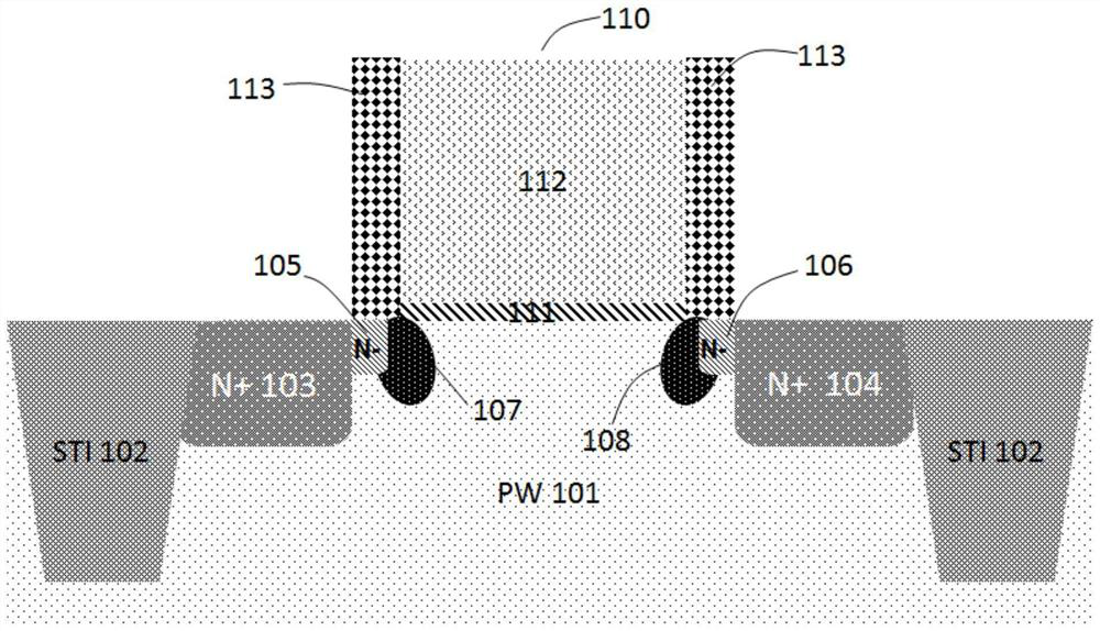
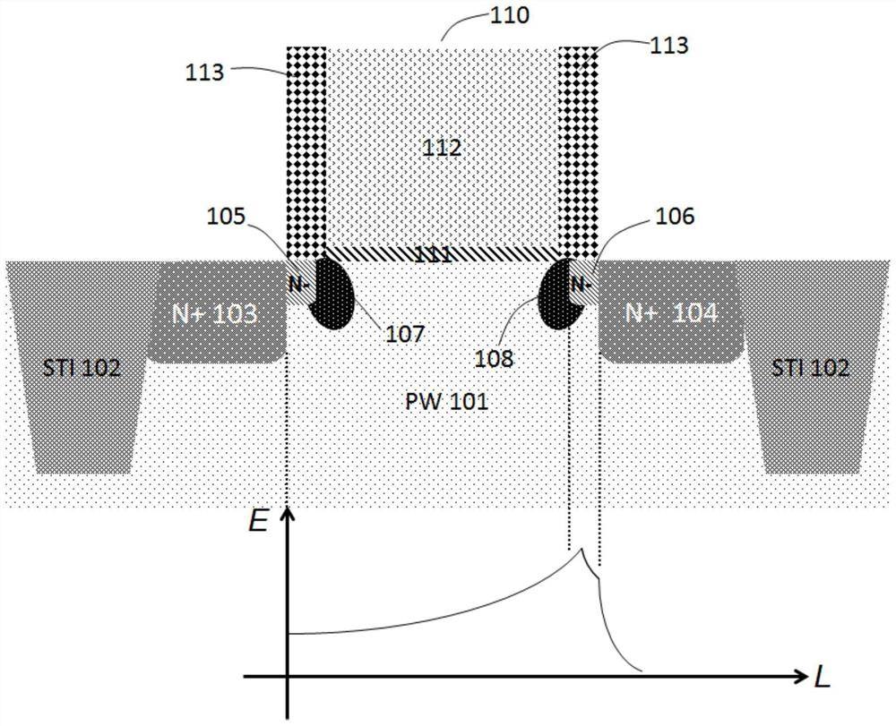
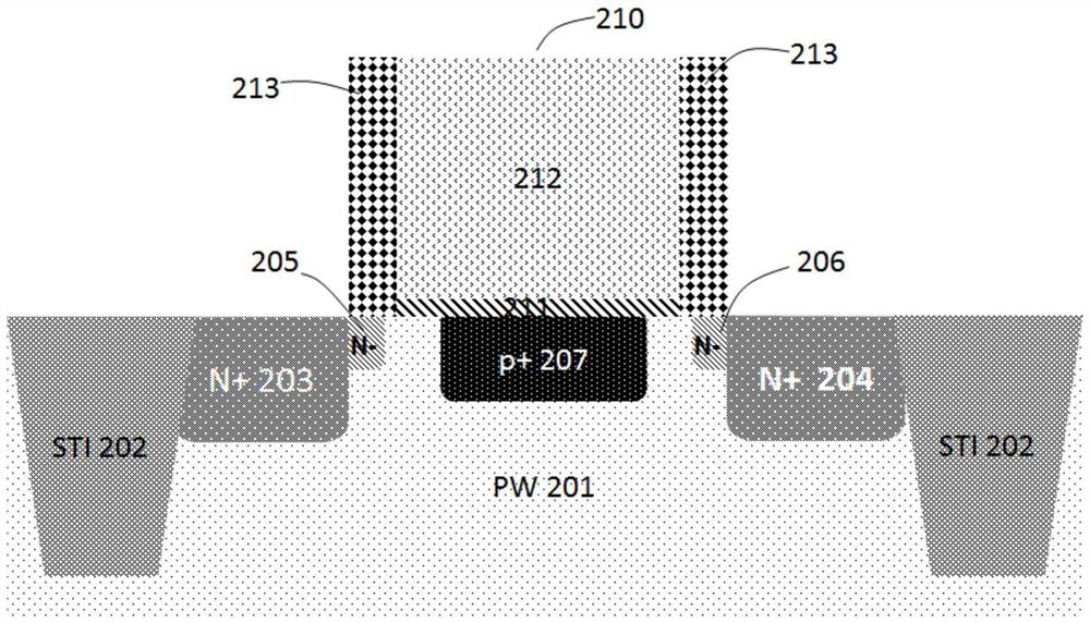
[0024] In one embodiment of the present invention, an NMOSFET device is provided. Specifically, see image 3 , image 3 It is a sche...


PUM


Abstract

The invention relates to a method for improving the hot carrier effect of an NMOSFET, belonging to a semiconductor integrated circuit technology. According to the method, a halo injection region is arranged between a lightly-doped drain region on the side of a source region and a lightly-doped drain region on the side of a drain region to form a central type halo injection region, so a section ofsubstrate Pwell doped region with a doping concentration lower than the doping concentration of the halo injection region is added between the halo injection region and the lightly-doped drain region;the lightly-doped drain region and the PW form a slowly-changing junction, and a depletion region extends into the central type halo injection region from the interface surface of the lightly-doped drain region and the PW, so an electric field can extend towards a channel direction again, and a peak electric field is further reduced; because the improved central type halo injection region structure has a more slowly-changing junction, the electric field can extend towards the channel direction, so the peak electric field is further reduced, electric field distribution is changed, and the purpose of further effectively improving HCI effect is finally achieved;and while the HCI effect is improved, the LDD structure of the central type halo injection region can effectively prevent short-channel effect.

Description

technical field [0001] The invention relates to semiconductor integrated circuit technology, in particular to a method for improving NMOSFET hot carrier effect. Background technique [0002] The device size of integrated circuits continues to shrink with the development of technology, which brings performance improvements and power consumption reductions. At the same time, the reliability problems caused by the shrinkage become increasingly severe. Among them, the channel lateral electric field strength of the device increases with the continuous shrinkage of the device size, especially the electric field near the drain is the strongest. When the feature size of the device is reduced to the sub-micron level, the hot carrier effect (Hot Carrier Inject, HCI) will appear near the drain. [0003] In order to improve the hot carrier injection effect, researchers have developed a light doped (LDD) process technology that reduces the peak electric field near the drain of the devic...

Claims


Application Information

Patent Timeline
Patent Type & Authority Applications(China)
IPC IPC(8): H01L29/78H01L29/06H01L29/36H01L21/336
CPCH01L29/0607H01L29/0684H01L29/36H01L29/66492H01L29/7833
Inventor 陆逸枫潘宗延陈明志
Owner SHANGHAI HUALI INTEGRATED CIRCUTE MFG CO LTD
Why Eureka
Try Eureka