Mixed order finite element method and device for triangular prism mesh generation of integrated circuit

An integrated circuit and grid subdivision technology, applied in special data processing applications, image data processing, 3D modeling, etc., can solve problems such as low computational efficiency, low computational efficiency, and no implementation method for transition units

Active Publication Date: 2020-12-25
北京智芯仿真科技有限公司
View PDF2 Cites 3 Cited by
  • Summary
  • Abstract
  • Description
  • Claims
  • Application Information

AI Technical Summary

Problems solved by technology

However, for a VLSI with a three-dimensional multi-scale structure, the grid refinement usually leads to an abnormal increase of the grid density in a large number of small-scale areas. The effect of increasing the calculation accuracy leads to low calculation efficiency; at the same time, due to the abnormal increase of the grid density in a large number of areas due to grid refinement, the overall number of grids has increased by tens of millions, which poses a challenge to the solution of the sparse matrix
Therefore, for 3D VLSI electromagnetic simulation, it is often used to increase the order of finite elements to improve calculation accuracy, such as increasing the first-order elements to second-order elements, but if all elements are increased to second-order elements, it will also lead to The unknown quantity of calculation increases sharply, but the calculation efficiency is still very low
In order to avoid raising all the units to the second-order unit and causing a sharp increase in the unknown quantity of calculation, it is proposed to use mixed-order finite elements. Based on the posterior error estimation, the second-order unit is used for the area with large error, and the first-order unit is used for other places. The area adjacent to the first-order unit and the second-order unit adopts a transition unit, but for the triangular prism unit, there is still no way to realize the transition unit

Method used


Image

  • Mixed order finite element method and device for triangular prism mesh generation of integrated circuit
  • Mixed order finite element method and device for triangular prism mesh generation of integrated circuit
  • Mixed order finite element method and device for triangular prism mesh generation of integrated circuit

Examples


Embodiment Construction

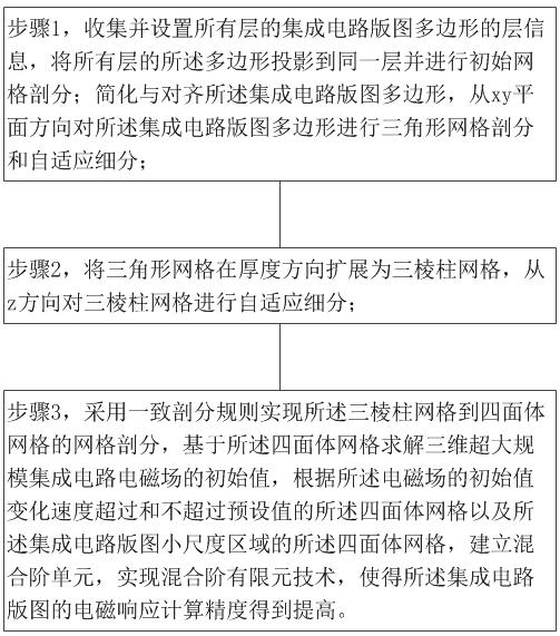
[0077] In order to make the objectives, technical solutions and advantages of the present invention clearer, the technical solutions in the embodiments of the present invention will be described in more detail below in conjunction with the drawings in the embodiments of the present invention.

[0078] It should be noted that: in the drawings, the same or similar symbols represent the same or similar elements or elements with the same or similar functions. The described embodiments are part of the embodiments of the present invention, but not all of the embodiments. In the case of no conflict, the embodiments in the present application and the features in the embodiments can be combined with each other. Based on the embodiments of the present invention, all other embodiments obtained by persons of ordinary skill in the art without creative efforts fall within the protection scope of the present invention.

[0079] In describing the present invention, it is to be understood that...


PUM


Abstract

The invention provides a mixed order finite element method and device for triangular prism mesh generation of an integrated circuit. The method comprises the steps of: collecting and setting layer information of polygons of an integrated circuit layout, projecting the polygons to the same layer, and performing initial mesh generation; simplifying and aligning the integrated circuit layout polygon,and performing triangular mesh generation and self-adaptive subdivision on the integrated circuit layout polygon from the xy direction; expanding the triangular mesh into a triangular prism mesh in the thickness direction, and performing adaptive subdivision on the triangular prism mesh in the z direction; adopting a consistent subdivision rule to realize subdivision from a triangular prism gridto a tetrahedral grid, and solving an initial value of a three-dimensional super-large-scale integrated circuit electromagnetic field based on the tetrahedral grid; and establishing a mixed order unitaccording to the tetrahedral mesh of which the initial value change speed of the electromagnetic field exceeds or does not exceed a preset value and the tetrahedral mesh of the small-scale region ofthe integrated circuit layout, thereby realizing a mixed order finite element technology. Rapid and high-quality triangular prism mesh generation is realized; and the electromagnetic response calculation precision is improved.

Description

technical field [0001] The invention relates to the technical field of integrated circuits, in particular to a mixed-order finite element method and device for triangular prism grid division of integrated circuits. Background technique [0002] With the rapid development of the integrated circuit industry, the traditional two-dimensional packaging technology has been unable to meet the increasing requirements of chip performance and packaging density, and three-dimensional packaging technology has become an irreversible trend of high-density chip packaging. A three-dimensional integrated circuit is to stack multiple planar chips vertically and interconnect them using gold wire bonding or other methods to form a three-dimensional packaging structure. Since the three-dimensional technology makes the most possible use of the three-dimensional space of the chip, more transistors can be packaged in a unit area in the form of stacking, which effectively reduces the delay and power...

Claims


Application Information

Patent Timeline
Patent Type & Authority Applications(China)
IPC IPC(8): G06F30/23G06T17/20
CPCG06T17/20G06F30/23
Inventor 唐章宏邹军王芬黄承清汲亚飞
Owner 北京智芯仿真科技有限公司
Why Eureka
Try Eureka