Compression ring assembly and semiconductor process chamber

A pressure ring and component technology, applied in semiconductor/solid-state device manufacturing, electrical components, discharge tubes, etc., can solve the problems of lower electrode structure damage, top breakage, control, etc., to reduce the probability of damage, reduce design difficulty, and reduce The effect of discharge

Pending Publication Date: 2020-12-29
BEIJING NAURA MICROELECTRONICS EQUIP CO LTD
View PDF0 Cites 0 Cited by
  • Summary
  • Abstract
  • Description
  • Claims
  • Application Information

AI Technical Summary

Problems solved by technology

[0004] However, during the lifting process of the above-mentioned pallet, due to the need for lifting cooperation between the thimble and the pressure ring, if the action sequence of the thimble and the pressure ring is wrong, it will cause the thimble to crush the pallet. The installation requires the assembly of multiple components such as bellows, lifting cylinders, needle bodies and adapters. However, the needle body, bellows, and some resin adapters are located in the strong electric field of the lower electrode structure. If the operation or installation If it is improper, there will be a discharge phenomenon with the lower electrode structure, which will cause damage to itself and the lower electrode structure, and because the thimble needs to penetrate the bottom wall of the reaction chamber, the base and the chuck, the design of the lower electrode structure is very complicated, and it is not conducive to Control the tightness of the reaction chamber

Method used


Image

  • Compression ring assembly and semiconductor process chamber
  • Compression ring assembly and semiconductor process chamber
  • Compression ring assembly and semiconductor process chamber

Examples


Embodiment Construction

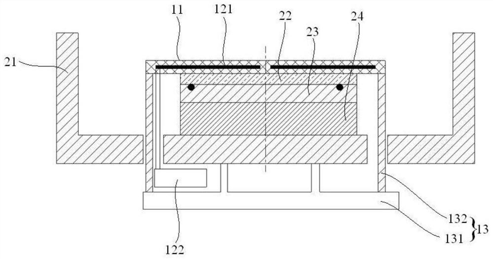
[0027] In order for those skilled in the art to better understand the technical solution of the present invention, the pressure ring assembly and the semiconductor process chamber provided by the present invention will be described in detail below with reference to the accompanying drawings.

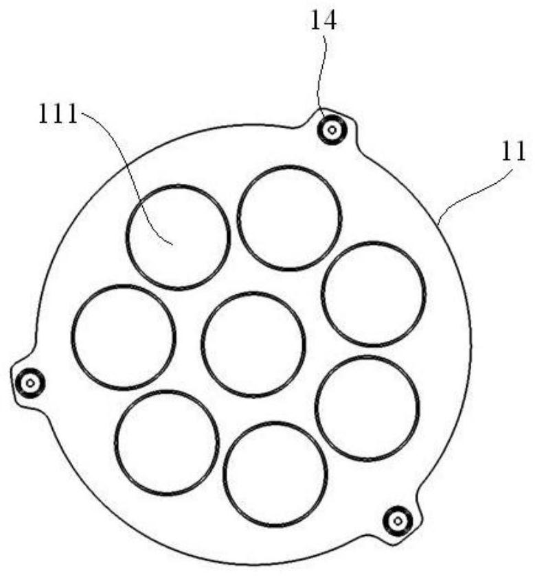
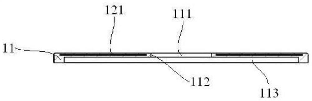
[0028] Such as figure 1 As shown, this embodiment provides a pressure ring assembly, the pressure ring assembly is used in conjunction with the chuck 23, the pressure ring assembly fixes the tray 22 on the chuck 23 through the lifting device 13, the pressure ring assembly includes an electrostatic assembly and an insulating pressure ring Ring body 11, wherein the pressure ring body 11 is used to contact the tray 22, and the pressure ring body 11 is provided with a through hole 111, and the through hole 111 is used to expose the wafer carried on the tray 22 (not shown in the figure); The electrostatic component is connected to the pressure ring body 11, and is used to cause the pressure r...


PUM


Abstract

The invention provides a compression ring assembly and a semiconductor process chamber, a compression ring is used in cooperation with a chuck, the compression ring fixes a tray to the chuck through alifting device, a compression ring assembly comprises an electrostatic assembly and an insulated compression ring body, the compression ring body is used for making contact with a tray, and through holes are formed in the compression ring body. The through holes are used for exposing wafers carried on the tray; the electrostatic assembly is connected with the compression ring body and used for enabling the compression ring body to generate electrostatic adsorption force so as to adsorb the tray through the compression ring body, and the electrostatic assembly is further used for eliminating the electrostatic adsorption force of the compression ring body so as to release the tray. According to the compression ring assembly and the semiconductor process chamber provided by the invention, the probability of damage to the tray can be reduced, the probability of occurrence of a discharge phenomenon can be reduced, the probability of damage to a lower electrode structure can be reduced, thedesign difficulty of the lower electrode structure can be reduced, and the sealing performance of a reaction chamber can be improved.

Description

technical field [0001] The invention relates to the technical field of semiconductor equipment, in particular to a pressure ring assembly and a semiconductor process chamber. Background technique [0002] Inductively coupled plasma (ICP) etching equipment usually has multiple chambers, and the manipulator needs to continuously transfer the tray carrying the wafer (Wafer) among the multiple chambers to complete the process. The entire etching process on the wafer. [0003] In the existing reaction chamber for etching process, there are usually a base, a chuck, a thimble and a pressure ring, wherein the base is arranged at the bottom of the reaction chamber, and the chuck is arranged on the base for It is used to carry the tray, and the base and the chuck are usually used as the lower electrode structure for attracting the plasma during the process. The thimble can be lifted and passed through the bottom wall of the reaction chamber, the base and the chuck. The pressure ring...

Claims


Application Information

Patent Timeline
Patent Type & Authority Applications(China)
IPC IPC(8): H01L21/683H01L21/687H01L21/67H01J37/305H01J37/32
CPCH01J37/3053H01J37/3056H01J37/321H01J37/32715H01J37/32752H01L21/67069H01L21/6831H01L21/6833H01L21/68742
Inventor 和长见张超
Owner BEIJING NAURA MICROELECTRONICS EQUIP CO LTD
Why Eureka
Try Eureka