Manufacturing method of three-dimensional memory and three-dimensional memory

A manufacturing method and memory technology, applied in the direction of electric solid-state devices, semiconductor devices, electrical components, etc., can solve problems such as cumbersome processes

Active Publication Date: 2021-01-05
YANGTZE MEMORY TECH CO LTD
View PDF4 Cites 4 Cited by
  • Summary
  • Abstract
  • Description
  • Claims
  • Application Information

AI Technical Summary

Problems solved by technology

[0003] However, in the current manufacturing method of the three-dimensional memory, when the thickness of the dummy gate covering layer in the step is increased through the additionally deposited dummy gate covering layer, not only the dummy gate covering layer deposited...

Method used


Image

  • Manufacturing method of three-dimensional memory and three-dimensional memory
  • Manufacturing method of three-dimensional memory and three-dimensional memory
  • Manufacturing method of three-dimensional memory and three-dimensional memory

Examples


Embodiment 1

[0063] The invention provides a method for manufacturing a three-dimensional memory, such as Figure 6 As shown, it includes the steps:

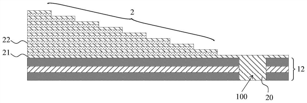
[0064] S1. Provide a substrate structure 1, define an array region 102 and edge regions 101, 103 in the substrate structure 1, the array region 102 includes a core region 1022 and step regions 1021, 1023;

[0065] S2, the semiconductor layer 12 on the substrate structure 1;

[0066] S3, forming a via hole 100 penetrating through the semiconductor layer 12 on the edge regions 101, 103, and filling the via hole 100 with the first dielectric layer 20;

[0067] S4, forming a stack structure 2' on the semiconductor layer 12 in the array region 102, the stack structure 2' comprising alternately stacked second dielectric layers 21 and dummy gate layers 22;

[0068] S5. Etching the stack structure 2' to form a step structure 2 on the step regions 1021 and 1023, the step structure 2 includes multiple steps 2a, and each step 2a includes a second die...

Embodiment 2

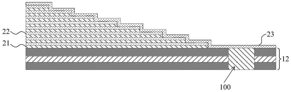
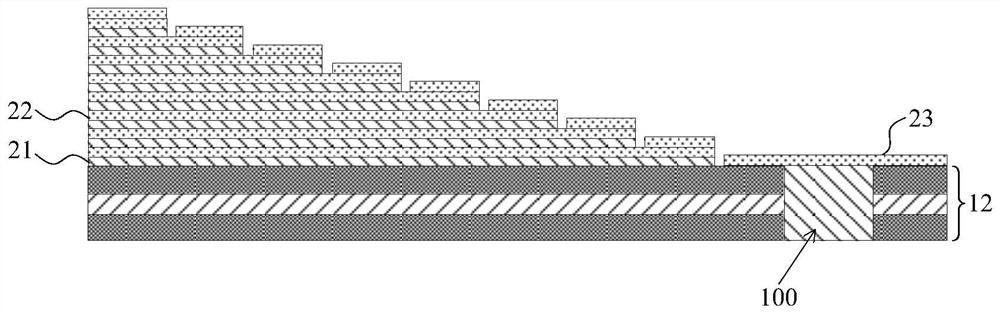
[0121] In Embodiment 1 of the present invention, as Figure 21 As shown, the etching of the first contact hole 200 stays on the dummy gate covering layer 23, that is, the first contact hole 200 does not pass through the dummy gate covering layer 23, but the etching of the corresponding third contact hole 500 is too much. etching; such as Figure 24 As shown, the second contact hole 400 and the third contact hole 500 are formed by simultaneous etching. After the fourth dielectric layer 26 is etched through, the semiconductor layer 12 needs to be used to fill the first dielectric in the first contact hole 200. The high selectivity ratio of layer 20 is achieved.

[0122]However, this has requirements on the material of the semiconductor layer 12 and the first dielectric layer 20 filled in the first contact hole 200 , and the etching depth of the corresponding second contact hole 400 is relatively deep, and the process conditions are relatively harsh.

[0123] Based on this, in ...


PUM


Abstract

The invention provides a manufacturing method of a three-dimensional memory and the three-dimensional memory, in the manufacturing method of the three-dimensional memory provided by the invention, after an additional pseudo gate covering layer is deposited on a step structure, only the pseudo gate covering layer on the side wall of the step is removed, and the residual pseudo gate covering layer on a semiconductor layer is not removed, instead, the dielectric layer is directly formed on the residual dummy gate covering layer and is etched and filled to form the metal plug, so that the etchingprocess is simplified, the mask is saved, the production efficiency is improved, and the production cost is reduced; meanwhile, when the contact hole is formed by etching, the etching which originallypasses through the contact hole of the semiconductor layer is changed to stay on the dummy gate covering layer, so that a corresponding etching window is reduced, and the design flexibility of the three-dimensional memory is enhanced.

Description

technical field [0001] The invention relates to the technical field of semiconductor manufacturing, in particular to a manufacturing method of a three-dimensional memory and a three-dimensional memory. Background technique [0002] Three-dimensional memory is a technology for stacking data units. At present, data units of 32 layers and above can be stacked. It overcomes the limitation of the actual expansion limit of planar memory, further increases the storage capacity, and reduces the storage cost of each data bit. , reducing energy consumption. [0003] However, in the current manufacturing method of the three-dimensional memory, when the thickness of the dummy gate covering layer in the step is increased through the additionally deposited dummy gate covering layer, not only the dummy gate covering layer deposited on the sidewall of the step needs to be removed, but also The dummy gate covering layer deposited on the semiconductor layer is removed, and the dummy gate cov...

Claims


Application Information

Patent Timeline
IPC IPC(8): H01L27/11568H01L27/11582
CPCH10B43/30H10B69/00H10B43/27
Inventor 张中吴林春张坤周文犀
Owner YANGTZE MEMORY TECH CO LTD
Why Eureka
Try Eureka