LCoS DISPLAY WITH A COLOR PIXEL ARRAY AND FABRICATION METHOD THEREOF

a technology of color pixel array and lcos display, which is applied in the field of refractive color lcos display, can solve the problems of high cost, difficult fabrication technology of micro color filter formed with inorganic dichroic materials, and inability to produce images from natural light or white light, green light, red, etc., and achieves the effect of simple fabrication process

Active Publication Date: 2008-11-27
UNITED MICROELECTRONICS CORP
View PDF4 Cites 4 Cited by
  • Summary
  • Abstract
  • Description
  • Claims
  • Application Information

AI Technical Summary

Benefits of technology

[0013]It is an advantage that the present invention provides a method to dispose reflective layers between different color filter layers and take the reflective layers as etching stop layers between color filter layers, such that simple etching processes can be used to define various patterns of color filter layers in various sub-pixels. Accordingly, the present invention can provide an LCOS panel with a color pixel array with simple fabrication process.

Problems solved by technology

As a result, in the conventional LCOS displays, it is rare that a LCOS panel has a color pixel array with different types color filter layers because the fabrication technology of the micro color filters formed with inorganic dichroic materials is difficult and has high cost.
Therefore, a single conventional LCOS panel cannot separate natural light or a white light source into primary color lights, the green light, red light, and blue light, or other color lights to produce images.
Therefore, the above-mentioned color wheel or color separation and combination optical system have to be used with several LCOS panels for generating colorful images, thus a conventional LCOS display with pluralities of LCOS panels and a complex optical engine has high fabrication cost and does not meet the market requirement of small-size products.
Accordingly, the fabrication method of color pixel array disclosed by lisaka is complicated and expensive, and his color filter structure is too thick to meet the small-size requirement of display market.
As a result, how to fabricate micro color filters with different colors or a color pixel array on a semiconductor substrate of a single LCOS panel through simple processes is still an important issue for LCOS display manufacturers.

Method used


Image

  • LCoS DISPLAY WITH A COLOR PIXEL ARRAY AND FABRICATION METHOD THEREOF
  • LCoS DISPLAY WITH A COLOR PIXEL ARRAY AND FABRICATION METHOD THEREOF
  • LCoS DISPLAY WITH A COLOR PIXEL ARRAY AND FABRICATION METHOD THEREOF

Examples


first embodiment

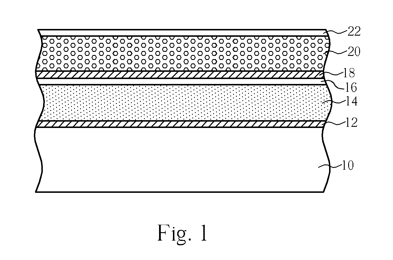
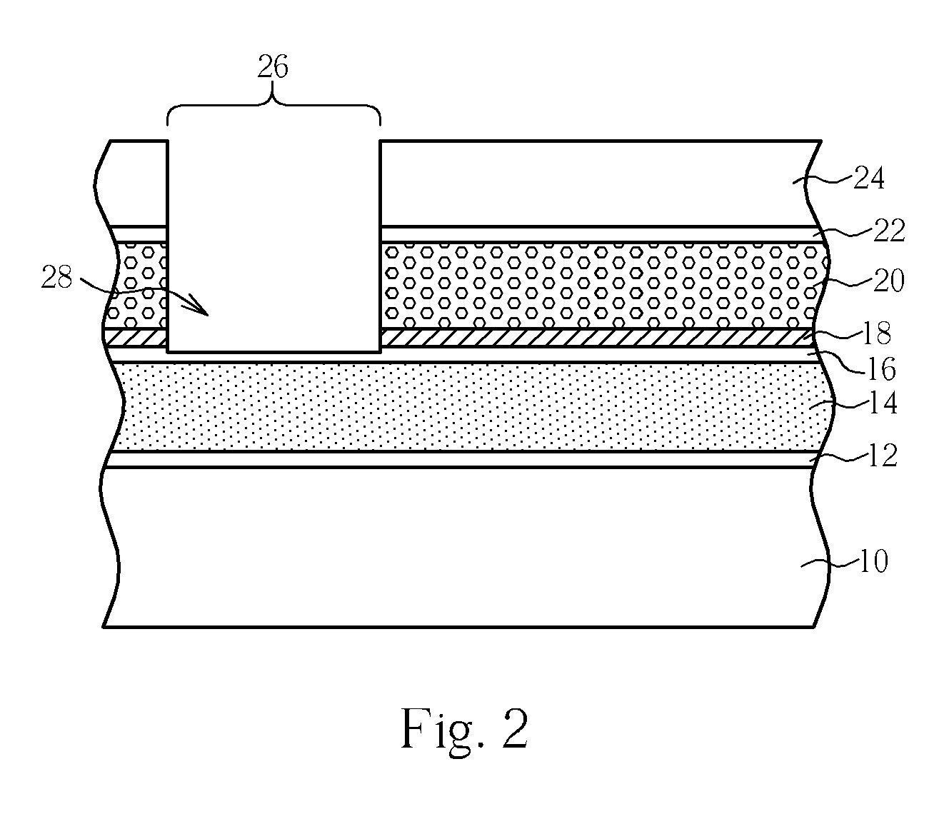
[0019]Please refer to FIGS. 1-7. FIGS. 1-7 are schematic diagrams of the fabrication method of an LCOS display with a color pixel array according to the present invention. In this embodiment, the present invention LCOS display is a reflective color LCOS display. As shown in FIG. 1, a semiconductor substrate 10, such as a silicon substrate, is provided, with a plurality of sub-pixel circuits and electric devices (not shown). Then, a first reflective layer 12, a first dichroic film 14, a first buffer layer 16, a second reflective layer 18, and a second dichroic film 20 are successively formed on the surface of the semiconductor substrate 10. The first and the second reflective layers 12, 18 may comprise conductive metal materials such that the first reflective layer 12 is capable of serving as a pixel electrode. The first dichroic film 14 and the second dichroic film 20 respectively serve as a first and a second color filter layers that may comprise high reflective films or dichroic m...

third embodiment

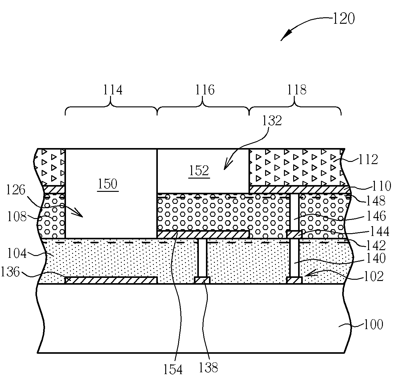
[0033]In other embodiments of the present invention, the first, second, and third dichroic films and the first, second, third reflective layers may be formed on the semiconductor substrate before performing etching processes to define the dichroic films or color filters. FIG. 14 to FIG. 19 are schematic diagrams of the fabrication method of an LCOS display with a color pixel array according to the present invention. First, as shown in FIG. 14, a semiconductor substrate 100 is provided. The semiconductor substrate 100 comprises a plurality of pixel circuits or electric devices (not shown) and a plurality of sub-pixels, such as the first sub-pixel 114, second sub-pixel 116, and third sub-pixel 118, for providing different kinds of color lights to form a color pixel array 120. Then, a first reflective layer 102, a first color filter layer 104, a second reflective layer 106, a second color filter layer 108, a third reflective layer 110, and a third color filter layer 112 are successivel...

second embodiment

[0039]In addition, although the method of forming the pixel electrodes and contact plugs between the first, second, and third color filter layers 104, 108, 112 are not taught in the second embodiment, those skilled in the art may combine the processes of the previous embodiments to form contact plugs, contact pads, or other electrical devices together with the present invention color pixel array 120. Furthermore, those skilled in the art may also combine the processes of the previous embodiments to provide a transparent substrate and liquid crystal molecules for combining with the semiconductor substrate 100 in order to form an LCOS display.


PUM

PropertyMeasurementUnit
conductiveaaaaaaaaaa
wavelengthsaaaaaaaaaa
transparentaaaaaaaaaa

Abstract

A method of fabricating an LCOS display with a color pixel array contains disposing reflective layers between various color filter layers. The reflective layers are used as etching stop layers between color filter layers so that etching processes are capable of carrying out to define the patterns of the color filter layers in different sub-pixels for forming the color pixel array.

Description

BACKGROUND OF THE INVENTION [0001]1. Field of the Invention[0002]The present invention relates to a colorful liquid crystal on silicon (LCOS) display, and more particularly, to a reflective color LCOS display.[0003]2. Description of the Prior Art[0004]LCOS display technology is the key of reflective LCOS projectors and rear-projection televisions. The advantages of LCOS micro-displays are a tiny size, high resolution, low power, low cost, etc. The difference between an LCOS display and a conventional thin film transistor-liquid crystal display (TFT-LCD) is materials used for forming the substrates. Both a cover substrate and a backplane are made of glass in a TFT-LCD. Nevertheless, the cover substrate in an LCOS display is made of glass, but the backplane in an LCOS display is a semiconductor substrate, such as silicon. Therefore, an LCOS process combines LCD techniques and complementary metal-oxide semiconductor (CMOS) fabrication processes.[0005]The main structure of an LCOS displ...

Claims


Application Information

Patent Timeline
Patent Type & Authority Applications(United States)
IPC IPC(8): G02F1/1335
CPCG02F1/133516G02F1/136277G02F2203/02
Inventor LIU, YAN-HSIU
Owner UNITED MICROELECTRONICS CORP
Why Eureka
Try Eureka