Hemi-spherical structure and method for fabricating the same

a hemispherical structure and hemispherical structure technology, applied in the direction of lenses, instruments, semiconductor/solid-state device details, etc., can solve the problems of insufficient curvature, insufficient curvature, and inability to control the uniformity, profile and curvature of the microlenses. uniformity,

Inactive Publication Date: 2007-07-05
TAIWAN SEMICON MFG CO LTD
View PDF7 Cites 4 Cited by
  • Summary
  • Abstract
  • Description
  • Claims
  • Application Information

AI Technical Summary

Benefits of technology

[0005] Embodiments of the present invention include hemi-spherical structures and methods of fabricating the

Problems solved by technology

One conventional method for manufacturing the microlens uses a thermal process and a blanket etch-back process to form a dielectric layer as a microlens array on a substrate, but has difficulties in controlling uniformity, profile and curvature of the microlenses. FIGS. 1A to 1D show conventional ladder etching process sequences for forming a microlens array.
This ladder etching process sequences, however,

Method used


Image

  • Hemi-spherical structure and method for fabricating the same
  • Hemi-spherical structure and method for fabricating the same
  • Hemi-spherical structure and method for fabricating the same

Examples


Embodiment Construction

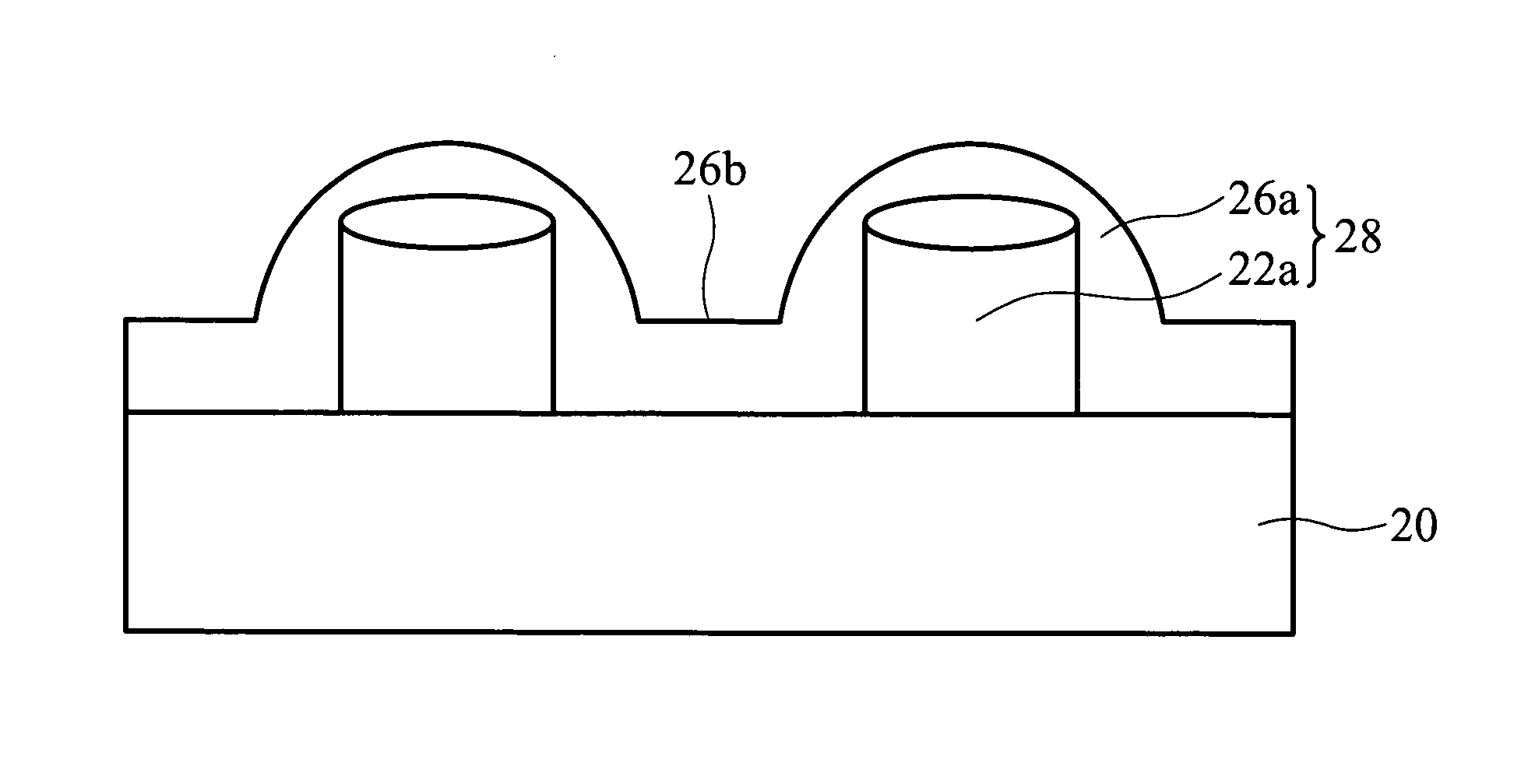
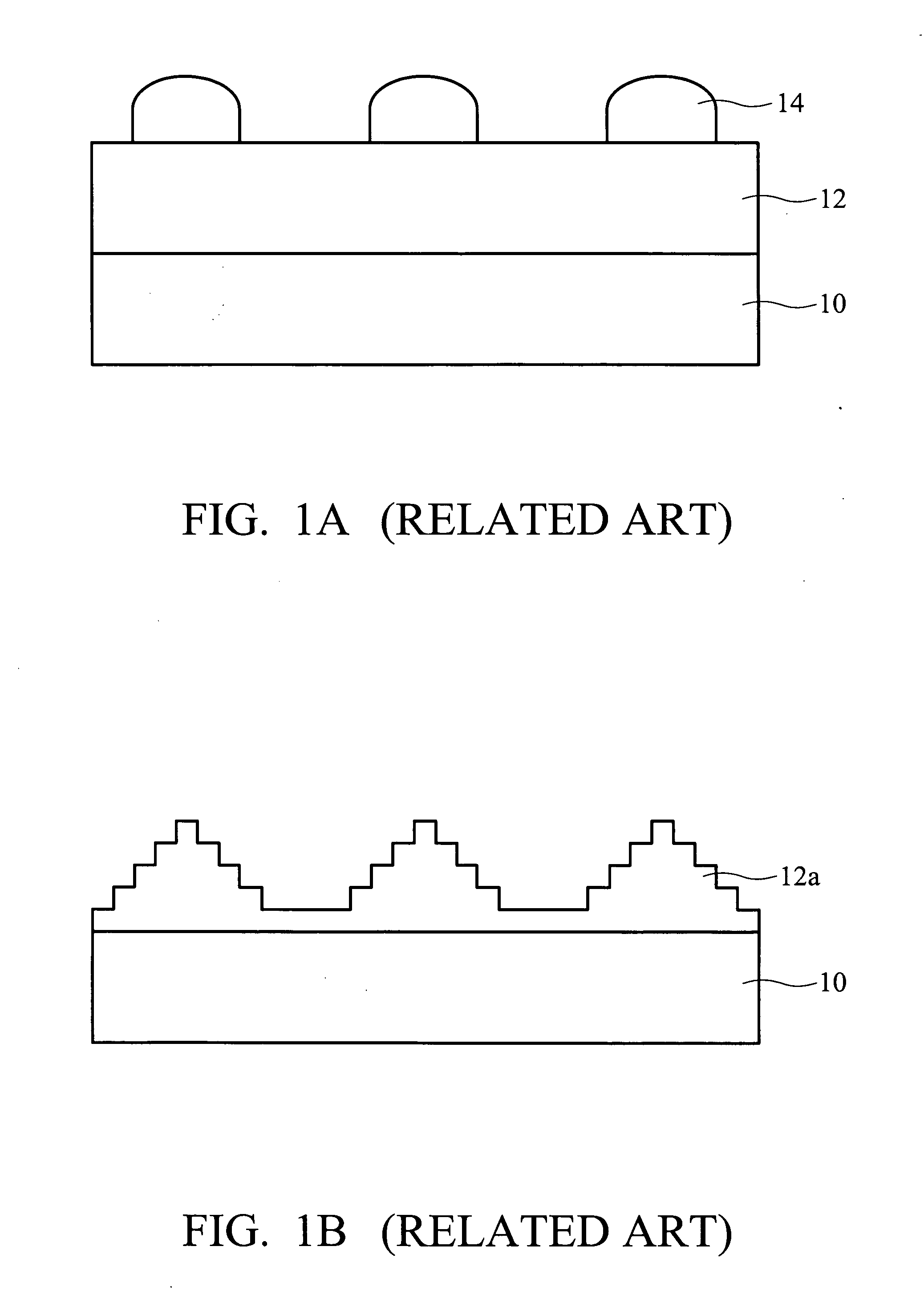
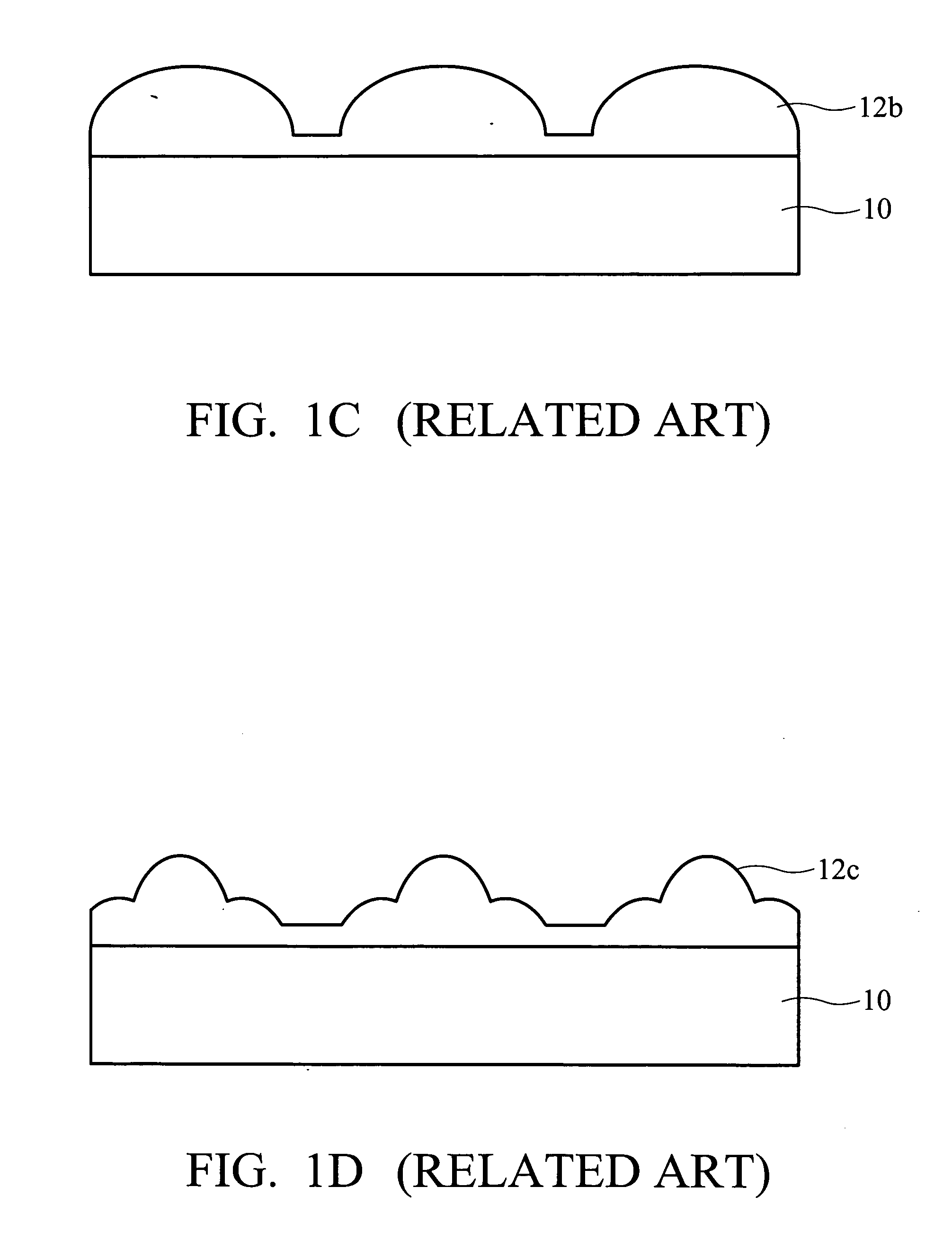
[0013] Embodiments of the present invention provide methods for fabricating hemi-spherical structures for use in optical information processing system, optical communication, optical pickup, optical measurement, and solid-sate image device applications. The hemi-spherical structure fabrication also adopts the Micro Electro-Mechanical System (MEMS) technology based upon the semiconductor processing to realize precision machining and more advantageous aspects in mass production. The inventive method can well control curvature, height and profile of the hemi-spherical structures to overcome the aforementioned problems of the conventional method through the use of a ladder etching process and a CDE process. Particularly, the present invention provides a hemi-spherical structure formed of inorganic or organic materials, which employs a support structure (e.g., a pillar region or a ladder-shaped region) under a hemi-spherical film region to control the height and curvature of the hemi-sph...


PUM


Abstract

Hemi-spherical structure and method for fabricating the same. A device includes discrete pillar regions on a substrate, and a pattern layer on the discrete support structures and the substrate. The pattern layer has hemi-spherical film regions on the discrete support structures respectively, and planarized portions on the substrate between the hemi-spherical film regions. Each of the hemi-spherical film regions in a position corresponding to each of the support structures serves as a hemi-spherical structure.

Description

TECHNICAL FIELD [0001] The present invention relates to hemi-spherical structures, and particularly to hemi-spherical structures for image device applications and micro-electro-mechanical-system technology and methods for fabricating the same. BACKGROUND [0002] Microlenses are widely used in various fields including an optical information processing system, an optical communication, an optical pickup, an optical measurement, or solid-sate image devices. Solid-state image devices typically include a photosensor such as a photodiode formed in or on a substrate, a color filter formed over the photosensitive device and a microlens array formed over the color filter. The photosensor may be a photodiode, a CMOS (complimentary metal oxide semiconductor) sensor or a charge-coupled device (CCD), for example. The function of the microlens is to efficiently collect incident light falling within the acceptance cone and refract this light in an image formation process onto a focal plane at a dep...

Claims


Application Information

Patent Timeline
IPC IPC(8): H01L21/84
CPCG02B3/0012B29D11/00278
Inventor LIU, MING-CHYILO, CHI-HSIN
Owner TAIWAN SEMICON MFG CO LTD
Why Eureka
Try Eureka