

Semiconductor laser packaging structure
A packaging structure and laser technology, applied in the direction of semiconductor lasers, lasers, laser components, etc., can solve the problems of chip temperature and cooler temperature rise, semiconductor laser temperature rise, heat cannot be taken away in time, etc.
- Summary
- Abstract
- Description
- Claims
- Application Information
AI Technical Summary
Problems solved by technology
Method used
Image

Examples
Embodiment 1
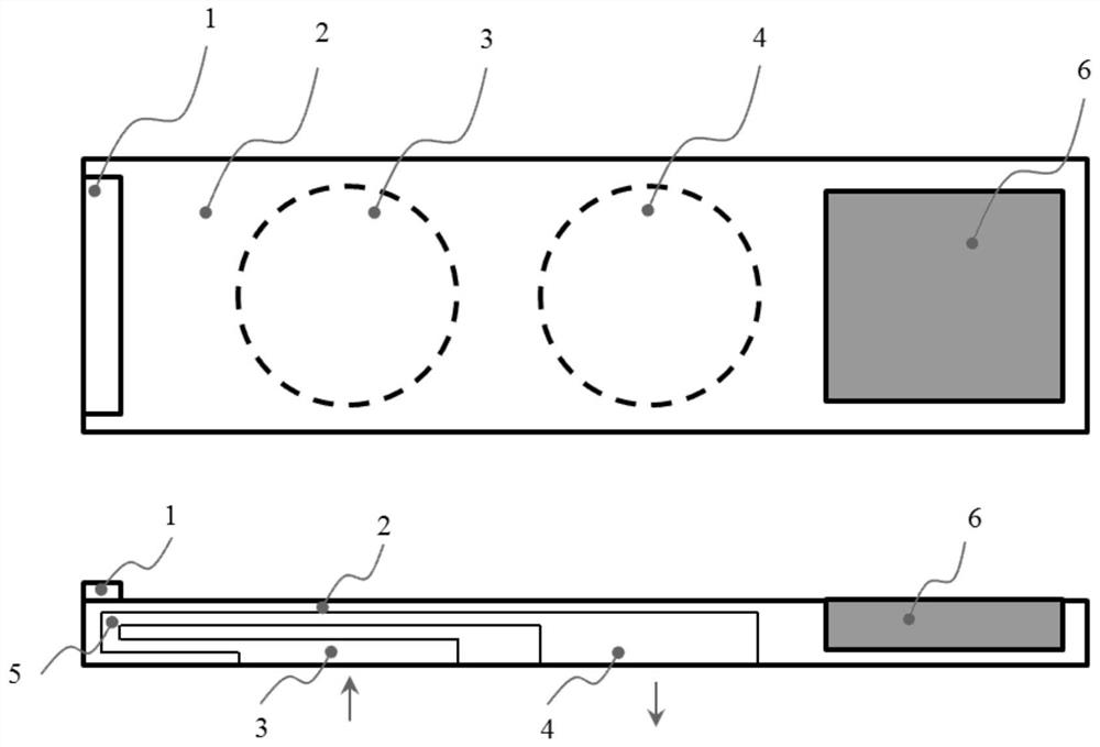
[0029] The first embodiment of the present invention provides a semiconductor laser packaging structure, such as figure 1 As shown, it includes a laser chip 1 and a cooler 2, and the laser chip 1 is packaged on the first outer surface of the cooler 2;
[0030] Wherein, the cooler 2 includes a coolant inlet 3, a coolant outlet 4, and a microchannel pipeline 5, and a phase change material 6 is encapsulated in the cooler 2, and when the semiconductor laser is in an abnormal working state, the phase change The material 6 is used to cool the temperature of the laser chip 1 below a preset safe temperature.
[0031] A phase change material (Phase Change Material, PCM) is usually a material that can undergo a phase change in a certain temperature range under normal pressure. Because solid-liquid phase change latent heat storage has the advantages of high heat storage density, the phase change process is approximately isothermal and the volume change is small, and the structure is rel...
Embodiment 2
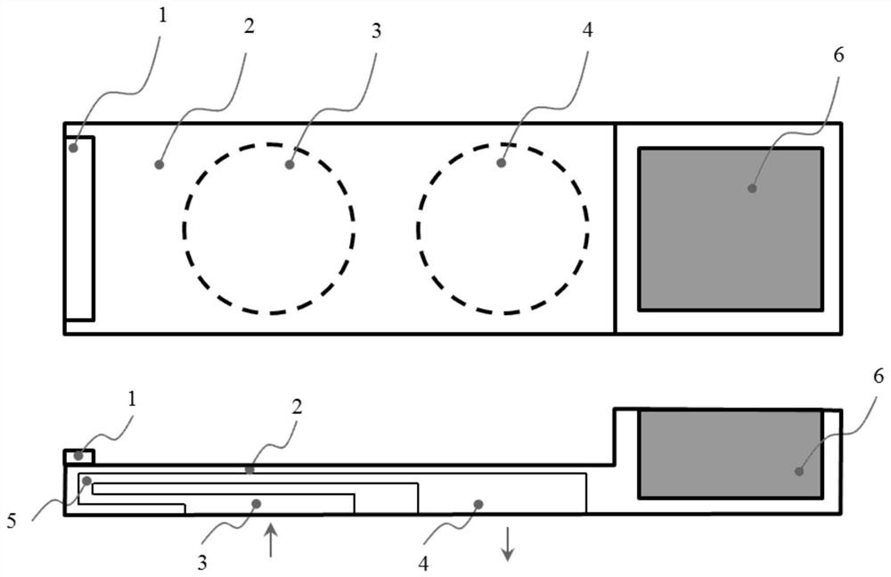
[0045] On the basis of Embodiment 1, in this embodiment, the packaging position of the phase change material 6 in the cooler 2 is illustrated. The phase change material 6 can be packaged at the end, both sides of the cooler, or any other suitable internal space. , and meet the requirements that the internal space of the packaged phase-change material 6 is isolated from the internal fluid channel of the cooler 2, as an optional implementation mode, the phase-change material 6 is packaged at the tail end of the cooler 2 for illustration in this embodiment.
[0046] An embodiment of the present invention provides a semiconductor laser packaging structure, such as figure 1 , figure 2 , image 3 As shown, it includes a laser chip 1 and a cooler 2, and the laser chip 1 is packaged on the first outer surface of the cooler 2;
[0047] Wherein, the cooler 2 includes a coolant inlet 3, a coolant outlet 4, and a microchannel pipeline 5, and a phase change material 6 is encapsulated in...
Embodiment 3
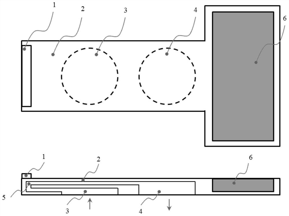
[0050] On the basis of Embodiment 1, in this embodiment, the packaging position of the phase change material 6 in the cooler 2 is illustrated. The phase change material 6 can be packaged at the end, both sides of the cooler, or any other suitable internal space. , and meet the requirement that the internal space of the packaged phase-change material 6 is isolated from the internal fluid channel of the cooler 2, as an optional implementation mode, in this embodiment, the phase-change material 6 is packaged around the cooler 2 for illustration.
[0051] An embodiment of the present invention provides a semiconductor laser packaging structure, such as Figure 4 As shown, it includes a laser chip 1 and a cooler 2, and the laser chip 1 is packaged on the first outer surface of the cooler 2;
[0052] Wherein, the cooler 2 is packaged with a phase-change material 6, and the phase-change material 6 is used to cool the temperature of the laser chip 1 below a preset safe temperature whe...
PUM
| Property | Measurement | Unit |
|---|---|---|
| phase transition enthalpy | aaaaa | aaaaa |
| density | aaaaa | aaaaa |
| melting point | aaaaa | aaaaa |
Abstract
Description
Claims
Application Information