Two-dimensional material detector based on asymmetric integration of optical microstrip antenna

A microstrip antenna, two-dimensional material technology, applied in the directions of antennas, resonant antennas, antenna components, etc., can solve the problems of low light absorption rate, complex conditions, and no absorption, and achieve strong process compatibility and simple process flow. , the effect of reducing costs

Active Publication Date: 2021-01-19
SHANGHAI INST OF TECHNICAL PHYSICS - CHINESE ACAD OF SCI
View PDF8 Cites 1 Cited by
  • Summary
  • Abstract
  • Description
  • Claims
  • Application Information

AI Technical Summary

Problems solved by technology

The problem of the former is that the heterojunction of two-dimensional materials is greatly affected by the different energy band structures and interfaces of heterogeneous materials, the situation is complicated, and it is difficult to effectively control the transport characteristics of carriers.
On the other hand, the ultra-thin thickness of 2D materials results in low light absorption; much light is reflected or transmitted, not absorbed

Method used


Image

  • Two-dimensional material detector based on asymmetric integration of optical microstrip antenna
  • Two-dimensional material detector based on asymmetric integration of optical microstrip antenna
  • Two-dimensional material detector based on asymmetric integration of optical microstrip antenna

Examples


Embodiment example

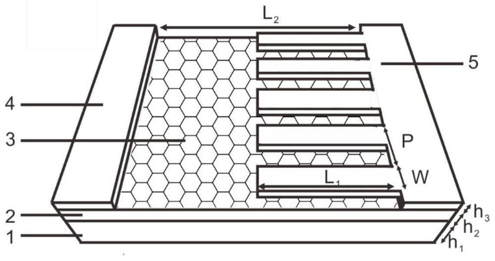
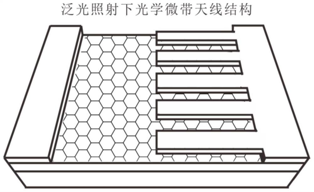
[0027] The asymmetrically integrated graphene detector of the optical microstrip antenna in this embodiment is aimed at a wavelength of 1.65 μm, and the metal is chromium / gold. The structural size of the periodic unit optimized by design is: P=590nm, W=283nm, L 1 =5μm,L 2 =10μm,h 1 =110nm,h 2 =30nm,h 3 = 45nm. Among them, the metal reflective layer 1 adopts Cr(20nm) / Au(90nm), the dielectric spacer layer 2 adopts Al2O3 which is transparent to the working band with a designed thickness as the dielectric layer, and the two-dimensional active material 3 is a copper-based material transferred by wet method. CVD-grown single-layer graphene, the source electrode 4 and the drain electrode 5 integrated with metal grid bars use Cr (5nm) / Au (45nm). As a control experiment, the general coupled grating asymmetrically integrated graphene device has the same top layer grating periodic structure size as the optical microstrip antenna asymmetrically integrated graphene detector, but its b...


PUM


Abstract

The invention discloses a two-dimensional material detector based on asymmetric integration of an optical microstrip antenna. The two-dimensional material detector structurally comprises a metal reflecting surface, a dielectric spacer layer, a two-dimensional active material layer and a drain electrode integrated by a top layer source electrode and a metal grid bar. The self-driven response of themetal optical detection structure of the metal two-dimensional active photosensitive material comes from a Schottky junction between the two-dimensional material and metal contact, the asymmetry integration of the optical microstrip antenna breaks the symmetry, the light absorption of the contact junction region of the two-dimensional material is greatly enhanced through the efficient coupling ofthe optical microstrip antenna and the light field local area. the boundary of the contact junction is prolonged, the light absorption of the two-dimensional material at the other electrode is inhibited by the metal bottom surface which is very close to the two electrodes, and the light response contrast ratio near the two electrodes is as high as more than one hundred times. Under floodlight irradiation, the responsivity of the optical microstrip antenna integrated two-dimensional material is higher than that of a traditional metal grating integrated two-dimensional material by more than oneorder of magnitude.

Description

technical field [0001] The invention relates to a two-dimensional material detector based on asymmetric integration of optical microstrip antennas, in particular to a two-dimensional material detector based on asymmetric integration of optical microstrip antennas and a design method for realizing self-driven optical response enhancement. Background technique [0002] At present, photodetectors are widely used in optical fiber communication, optical imaging, remote sensing, and biomedical analysis systems, and have become an indispensable part of daily life. However, among many photodetectors, each detector must meet certain requirements before it can be applied in relevant industries and researches. Due to the different operating wavelength requirements, the energy bandgap of the semiconductor material used to fabricate the photodetector must be carefully selected to match the corresponding operating wavelength. Over the past decade, emerging 2D layered materials have spurr...

Claims


Application Information

Patent Timeline
Patent Type & Authority Applications(China)
IPC IPC(8): H01L31/101H01L31/0232H01Q1/22
CPCH01L31/101H01L31/02327H01Q1/2283H01L31/035209H01L31/112H01L31/0224H01L31/1013H01Q9/0407
Inventor 周靖郭尚坤余宇嵇兆煜代旭邓杰陈效双蔡清元储泽世李方哲兰梦珂
Owner SHANGHAI INST OF TECHNICAL PHYSICS - CHINESE ACAD OF SCI
Why Eureka
Try Eureka