Data rate bit-by-bit variable digital-to-analog conversion device and configuration method

A technology of digital-to-analog conversion and data rate, applied in the direction of digital-to-analog converters, etc., can solve problems such as high cost, complex hardware circuit, and inability to realize self-adaptive configuration, and achieve the goal of reducing storage space, simplifying design, and simplifying hardware circuit design Effect

Active Publication Date: 2021-01-19
NO 54 INST OF CHINA ELECTRONICS SCI & TECH GRP
View PDF3 Cites 0 Cited by
  • Summary
  • Abstract
  • Description
  • Claims
  • Application Information

AI Technical Summary

Problems solved by technology

At present, a digital-to-analog conversion device with a bit-by-bit variable data rate based on a dedicated digital-to-analog conversion chip requires an additional clock management chip to provide a clock, which is costly and complex in hardware circuits
However, for the digital-to-analog conversion device based on the AD9361 RF agile transceiver, once the data rate is switched, the parameter values ​​​​of the clock configuration function need to be recalculated according to its design restrictions, and adaptive configuration cannot be realized.

Method used


Image

  • Data rate bit-by-bit variable digital-to-analog conversion device and configuration method
  • Data rate bit-by-bit variable digital-to-analog conversion device and configuration method

Examples


Embodiment Construction

[0032] In order to make it easier for those skilled in the art to understand the technical solution of this patent, and at the same time, in order to make the technical purpose, technical solution and beneficial effect of this patent clearer, and to fully support the protection scope of the claims, the following is a specific case in the form of this patent. The technical solution of the patent makes further and more detailed descriptions.

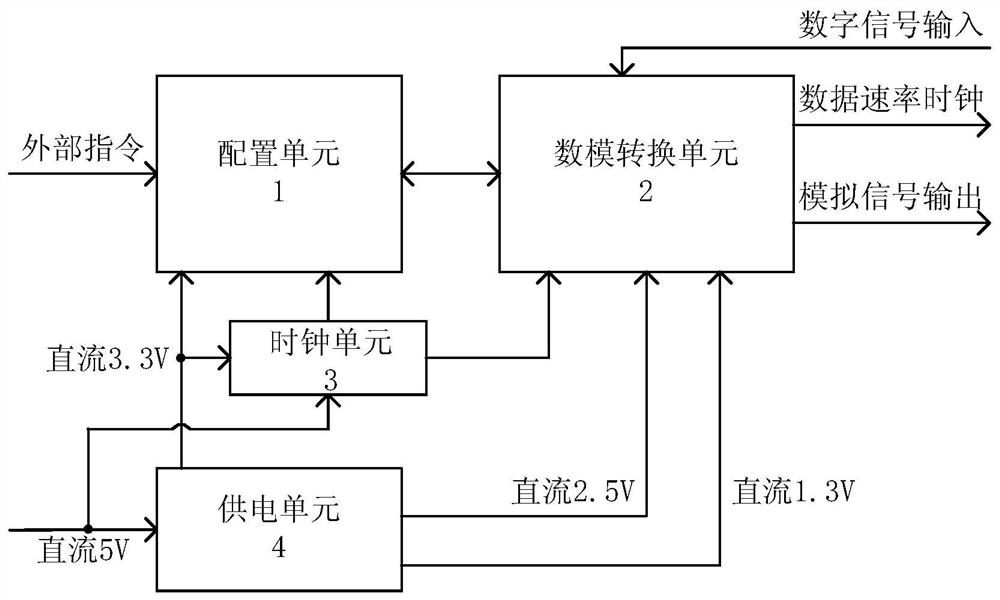
[0033] refer to figure 1 , a digital-to-analog conversion device with variable data rate bit by bit, which includes a configuration unit 1 , a digital-to-analog conversion unit 2 , a clock unit 3 , and a power supply unit 4 . figure 1 It is a block diagram of the hardware design principle of the present invention, and the embodiment is according to figure 1 Connect the lines.

[0034] Among them, the power supply unit divides the DC 1.3V, 2.5V, and 3.3V from the internal two power supply chips according to the external input DC 5V power ...


PUM


Abstract

The invention discloses a data rate bit-by-bit variable digital-to-analog conversion device and a configuration method, and belongs to the technical field of digital-to-analog conversion. The device comprises a configuration unit, a digital-to-analog conversion unit, a clock unit, a power supply unit, and a table lookup unit, a storage unit, an operation unit and a parameter configuration unit which are realized in a software module form. The configuration unit is used for configuring the data rate clock of the analog-to-digital conversion unit to be rapidly switched within the stepping rangeof 1Hz and the range of 1MHz-125MHz. The digital-to-analog conversion unit outputs a required data rate clock according to the control instruction. The clock unit provides 8MHz and 50MHz reference clock sources for the configuration unit and the digital-to-analog conversion unit respectively. The power supply unit supplies required direct-current power to the configuration unit, the digital-to-analog conversion unit and the clock unit. The device has the advantages of being simple in hardware circuit, low in cost, simple in configuration algorithm structure, small in occupied resource and capable of achieving self-adaptive switching.

Description

technical field [0001] The invention relates to the technical field of digital-to-analog conversion, in particular to a digital-to-analog conversion device and a configuration method with variable data rate bit by bit. Background technique [0002] Faced with the situation of diversified functions, integrated functions, and miniaturized equipment in the field of mobile communication and satellite communication, the modem needs to integrate more functions under the premise of miniaturized equipment, especially a communication system that covers a wider range of data rates. The AD9361 RF Agile Transceiver encapsulates its signal chain in a software-configurable IC, and has been widely used in the communication field due to its configurability, low power consumption, and small size. At present, a bit-by-bit variable digital-to-analog conversion device based on a dedicated digital-to-analog conversion chip requires an additional clock management chip to provide a clock, which is...

Claims


Application Information

Patent Timeline
Patent Type & Authority Applications(China)
IPC IPC(8): H03M1/66
CPCH03M1/66
Inventor 孙南南汪颜张隽康尚国武
Owner NO 54 INST OF CHINA ELECTRONICS SCI & TECH GRP
Why Eureka
Try Eureka