
Display panel and preparation method thereof

A display panel and metal technology, which is applied in the direction of electrical components, transistors, electric solid devices, etc., can solve the problem of low adhesion between the metal oxide layer and the Cu film, achieve the effect of preventing peeling off and improving the yield rate

Active Publication Date: 2021-01-22
TCL CHINA STAR OPTOELECTRONICS TECH CO LTD
View PDF8 Cites 0 Cited by
  • Summary
  • Abstract
  • Description
  • Claims
  • Application Information

AI Technical Summary

Problems solved by technology

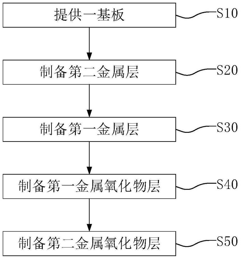
[0004] The purpose of the present invention is to provide a display panel and a preparation method thereof, to solve the problem of low adhesion between the low reflection metal oxide layer and the Cu film in the prior art

Method used


Image

  • Display panel and preparation method thereof
  • Display panel and preparation method thereof
  • Display panel and preparation method thereof

Examples


Embodiment 1

[0044] An embodiment of the present invention provides a display device, which has a display panel 100, and the display panel 100 is used to provide a display image for the display device. The display device can be any product or component with a display function, such as a mobile phone, a tablet computer, a notebook computer, and the like.

[0045] like Figure 5 As shown, the display panel 100 has a substrate 10 , a first metal layer 20 , a second metal layer 40 and a metal oxide layer 30 .

[0046] The substrate 10 is used to protect the overall structure of the display panel 100 , which may be an insulating substrate such as a glass substrate or a quartz substrate.

[0047] The first metal layer 20 is disposed on a surface of the substrate 10 and is used for transmitting electric energy for devices in the display panel 100 . The first metal layer 20 is made of a metal material with excellent electrical conductivity, and the metal material may be copper.

[0048] The secon...

Embodiment 2

[0064] An embodiment of the present invention provides a display device, which has a display panel 100, and the display panel 100 is used to provide a display image for the display device. The display device can be any product or component with a display function, such as a mobile phone, a tablet computer, a notebook computer, and the like.

[0065] like Figure 9 As shown, the display panel 100 has a substrate 10 , a first metal layer 20 and a metal oxide layer 30 .

[0066] The substrate 10 is used to protect the overall structure of the display panel 100 , which may be an insulating substrate such as a glass substrate or a quartz substrate.

[0067] The first metal layer 20 is disposed on the substrate 10 and is used for transmitting electric energy for devices in the display panel 100 . The first metal layer 20 is made of a metal material with excellent electrical conductivity, and the metal material may be copper.

[0068] The metal oxide layer 30 is disposed between t...


PUM


Abstract

The invention provides a display panel and a preparation method thereof. The display panel comprises a first metal layer and at least two metal oxide layers. The metal oxide layers are stacked on onesurface of the first metal layer. In the metal oxide layers, the content of oxygen atoms in metal oxide gradually decreases from the side away from the metal layer to the side close to the metal layer.

Description

technical field [0001] The invention relates to the field of display devices, in particular to a display panel and a preparation method thereof. Background technique [0002] In the current large-size display panel products, especially the current hot 8K products, the conductive layer (such as the gate) in the TFT (Thin Film Transistor, thin film transistor) panel is generally made of Cu (copper) and other metals. However, the reflectance of visible light on the surface of the Cu film can reach up to 90%, and the Cu film is not shielded above. When the visible light reaches the surface of the Cu film, it will be reflected, resulting in high reflectance of the product and affecting the visual effect. [0003] Designing a low-reflectivity molybdenum oxide layer above or below the Cu film can reduce the reflectivity of the product and meet the needs of high-end products. However, molybdenum oxide has an amorphous structure and poor adhesion to Cu. Direct contact, after subsequ...

Claims


Application Information

Patent Timeline
Patent Type & Authority Applications(China)
IPC IPC(8): H01L27/12H01L29/423H01L29/786
CPCH01L27/1214H01L27/1259H01L29/4238H01L29/786
Inventor 胡小波
Owner TCL CHINA STAR OPTOELECTRONICS TECH CO LTD
Learn More