
A kind of semiconductor laser and its manufacturing method
A laser and semiconductor technology, applied in the direction of semiconductor lasers, lasers, laser components, etc., can solve problems affecting the use of semiconductor lasers, reduce fiber coupling efficiency, unfavorable beam adjustment, etc., increase the size of the vertical direction of the spot, improve fiber coupling efficiency , Improve the effect of output quality
- Summary
- Abstract
- Description
- Claims
- Application Information
AI Technical Summary
Problems solved by technology
Method used
Image

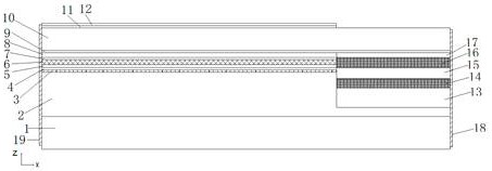
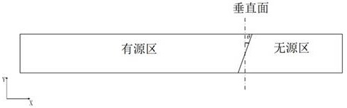
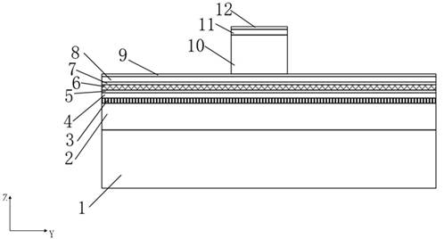
Examples
Embodiment Construction
[0034] The technical solutions in the embodiments of the present invention will be clearly and completely described below with reference to the accompanying drawings in the embodiments of the present invention. Obviously, the described embodiments are only a part of the embodiments of the present invention, not all of the embodiments. Based on the embodiments of the present invention, all other embodiments obtained by those of ordinary skill in the art without creative efforts shall fall within the protection scope of the present invention.
[0035] In the following examples, the figure 1 to the attached Figure 8 The x direction is the length direction of the resonant cavity, that is, the length direction of each layer; the Y direction is the width direction of the resonant cavity, that is, the width direction of each layer; the Z direction is the height direction of the resonant cavity, which is also the vertical direction.
[0036] First, as figure 1 , image 3 and Fig...
PUM
| Property | Measurement | Unit |
|---|---|---|
| length | aaaaa | aaaaa |
| length | aaaaa | aaaaa |
| thickness | aaaaa | aaaaa |
Abstract
Description
Claims
Application Information