Carrier for MEMS chip technological processing

A process and carrier technology, applied in the field of carriers for MEMS chip process processing, can solve problems such as low yield, inaccurate positioning, and difficulty in fixing

Pending Publication Date: 2021-02-02
WUXI RED MICROELECTRONICS CORP
View PDF0 Cites 0 Cited by
  • Summary
  • Abstract
  • Description
  • Claims
  • Application Information

AI Technical Summary

Problems solved by technology

[0003] Aiming at the problem of inaccurate positioning and difficulty in fixing the existing MEMS chip during the process of reflow soldering and housing installation, resulting in a low yield rate, the present invention provides a carrier for MEMS chip processing, which can fix the MEMS chip Installed on the carrier, the MEMS chip is positioned accurately and fixed firmly, thereby improving the yield rate of the product

Method used


Image

  • Carrier for MEMS chip technological processing
  • Carrier for MEMS chip technological processing
  • Carrier for MEMS chip technological processing

Examples


Embodiment Construction

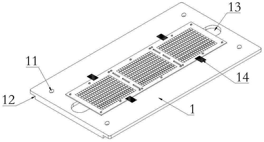
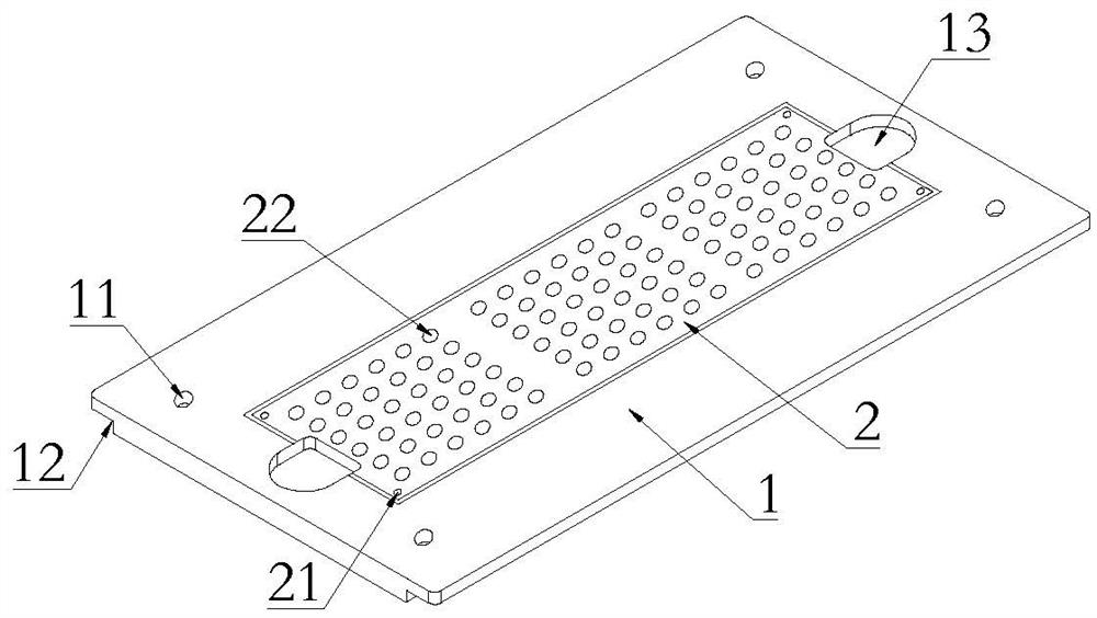
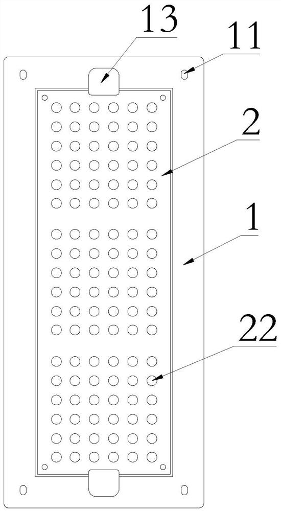
[0014] Such as Figure 1 to Figure 3 Shown, a kind of carrier for MEMS chip technology processing comprises carrier body 1, and the surface of carrier body 1 is provided with the profiling area 2 corresponding with MEMS chip 3 profiles, by this profiling area 2 MEMS chip is placed on top. Preferably, the profiling area 2 can be provided on the carrier body 1 with a rectangular wire frame matching the shape of the MEMS chip 3; or the profiling area 2 can be provided on the carrier body 1 A rectangular groove matching the shape of the MEMS chip 3 , the depth of the rectangular groove is slightly greater than the thickness of the MEMS chip 3 .

[0015] The four corners of the profiling area 2 are respectively provided with first positioning holes 21 corresponding to the holes in the four corners of the MEMS chip 3 . The MEMS chip 3 is accurately positioned through the first positioning hole 21 . The profiling area 2 is also provided with a through hole group 22, and the throug...


PUM


Abstract

According to the carrier for MEMS chip technological processing provided by the invention, the MEMS chip can be fixedly mounted on the carrier, so that the MEMS chip is accurately positioned and stably fixed, and the yield of products is improved. The carrier comprises a carrier body and is characterized in that the surface of the carrier body is provided with profiling areas corresponding to theshapes of MEMS chips, the profiling areas are provided with first positioning holes corresponding to holes of the MEMS chips respectively, the profiling areas are further provided with through hole sets, through holes in the through hole sets correspond to pins of the MEMS chips respectively. Second positioning holes are formed in the positions of the carrier body respectively, and notches extending inwards are formed in the edges of the two long side edges of the bottom of the carrier body respectively.

Description

technical field [0001] The invention relates to the technical field of MEMS chip processing tooling, in particular to a carrier for MEMS chip processing. Background technique [0002] MEMS is the abbreviation of Micro-Electro-Mechanical System. The Chinese name is micro-electro-mechanical system. MEMS chip is to use semiconductor technology to manufacture electro-mechanical systems on silicon chips. During the processing of existing MEMS chips, when processing to the reflow soldering step, the MEMS chips are placed on the conveyor belt and transported to the reflow soldering machine for welding. However, since the MEMS chips are directly placed on the conveyor belt, and because The high temperature of welding is easy to make the MEMS chip have a certain degree of curvature, which makes it difficult to position the MEMS chip accurately, and it is easy to offset the soldering of the pins of the MEMS chip, resulting in an increase in the defect rate; A shell is installed on th...

Claims


Application Information

Patent Timeline
Patent Type & Authority Applications(China)
IPC IPC(8): B81C99/00B23K3/08
CPCB23K3/087B81C99/0005
Inventor 侯友良
Owner WUXI RED MICROELECTRONICS CORP
Why Eureka
Try Eureka