Packaging device, preparation method thereof and electronic equipment

A technology for packaging devices and electronic components, which is applied in the field of electronics and can solve the problems of increasing the area of ​​packaging devices and detrimental to the lightweight of electronic equipment.

Active Publication Date: 2021-02-02
HUAWEI TECH CO LTD
View PDF13 Cites 4 Cited by
  • Summary
  • Abstract
  • Description
  • Claims
  • Application Information

AI Technical Summary

Problems solved by technology

[0006] The embodiment of the present application provides a packaged device and its preparation method, and electronic equipment, which are used to solve the problem that th...

Method used


Image

  • Packaging device, preparation method thereof and electronic equipment
  • Packaging device, preparation method thereof and electronic equipment
  • Packaging device, preparation method thereof and electronic equipment

Examples


example 1

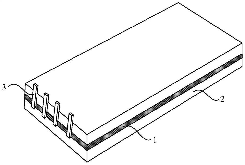
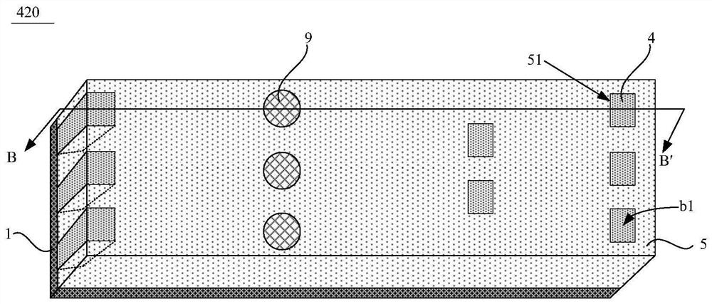
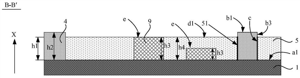
[0087] like image 3 As shown, the packaging device 420 includes a circuit board 1 , a first pin 4 , a first electronic component 9 , and a first plastic packaging layer 5 .

[0088] The circuit board 1 has a first surface a1.

[0089] The first plastic sealing layer 5 covers the first surface a1 ; the first plastic sealing layer 5 includes at least one first channel 51 , and the first channel 51 penetrates the first plastic sealing layer 5 along the first direction X.

[0090] The first channel 51 is a through hole, and the first channel 51 is located in the area surrounded by the side d2 of the first plastic sealing layer 5 .

[0091] It can be understood that the first passage 51 here is a through hole relative to the first molding layer 5 , that is to say, the first passage 51 penetrates the first molding layer 5 . However, for the entire packaged device, the first channel 51 is a blind hole, and the first channel 51 does not penetrate the circuit board 1 . Wherein, the...

example 2

[0123] like Figure 8a and Figure 8b (along Figure 8a As shown in the cross-sectional view in the D-D' direction), the difference between the second example and the first example is that the first passage 51 for placing the first pin 4 includes a connected first sub-channel 511 and a second sub-channel 512. The second sub-channel 512 is arranged closer to the circuit board 1 than the first sub-channel 511 .

[0124] like Figure 9a As shown, the first pin 4 and the first electronic component 9 are independently arranged in a first channel 51 .

[0125] like Figure 9b (along Figure 9a As shown in the cross-sectional view in the E-E' direction), there is a gap z between the surface of the first pin 4 facing the inner wall c1 of the first sub-channel 511 and the inner wall c1 of the first sub-channel 511 .

[0126] In some implementation manners, the above-mentioned gap z can be formed on the basis of the first plastic encapsulation layer 5 of Example 1 by means of lase...

example 3

[0134] like Figure 11a As shown, the difference between Example 3 and Example 1 and Example 2 is that the first channel 51 is a through groove, and the first channel 51 is located on the side d2 of the first plastic sealing layer 5 .

[0135] In this case, the groove wall c of the through groove serves as a side d2 of a part of the first plastic sealing layer 5 .

[0136] The side d2 of the first plastic encapsulation layer 5 not only intersects the first surface a1 , but also intersects the upper surface d1 of the first plastic encapsulation layer 5 away from the circuit board 1 .

[0137] In some embodiments, such as Figure 11a As shown, along the first direction X, the cross-sectional area of ​​the through groove does not change. like Figure 11b (along Figure 11a As shown in the view in the Y direction), along the first direction X, the projection of the groove wall of the through groove is two parallel lines.

[0138] In some embodiments, such as Figure 12a As s...


PUM


Abstract

The invention provides a packaging device, a preparation method thereof and electronic equipment, relates to the technical field of electronics, and is used for solving the problems that the area of the packaging device is increased and the lightness of the electronic equipment is not facilitated due to the fact that pins of the packaging device are located on the side surface. The packaging device includes a circuit board, a first plastic package layer and at least one first pin, wherein the circuit board is provided with a first surface; the first plastic package layer covers the first surface, the first plastic package layer comprises at least one first channel, the first channel penetrates through the first plastic package layer in a first direction, and the first direction is perpendicular to the first surface; and the at least one first pin is electrically connected with the circuit board, one first pin is located in one first channel, at least part of the first pin is connectedwith the inner wall of the first channel, the first channel is exposed out of the first conductive surface, which is away from the circuit board, of the first pin, and the first pin is electrically connected with an external device through the first conductive surface.

Description

technical field [0001] The present application relates to the field of electronic technology, in particular to a packaging device, a preparation method thereof, and electronic equipment. Background technique [0002] With the rapid development of science and technology, communication equipment such as mobile phones, computers, tablets, and base stations have become popular. In order to improve product performance and competitiveness, various communication equipment manufacturers have designed electronic components in communication equipment, such as packaging devices. Higher demands are placed on production as well as performance. [0003] like figure 1 As shown, the packaging device generally includes a circuit board 1 , a plastic sealing layer 2 covering the upper surface and the lower surface of the circuit board 1 , and pins 3 arranged on the side of the circuit board 1 . [0004] figure 1 The manufacturing process of the packaged device shown is as follows: first pac...

Claims


Application Information

Patent Timeline
IPC IPC(8): H01L23/31H01L23/48H01L23/49
CPCH01L23/3121H01L23/48H01L23/49H01L2924/181H01L2924/1815H01L2924/1304H01L2924/1203H01L2924/19043H01L2924/19042H01L2924/19041H01L2224/29101H01L2224/32225H01L2224/83801H01L24/29H01L24/32H01L24/83H01L23/49811H01L21/56H01L21/561H01L23/562H01L21/565H01L2224/97H01L2924/00012H01L2924/014H01L2924/00014H01L2224/83H01L21/60
Inventor 潘伟健胡志祥叶刚
Owner HUAWEI TECH CO LTD
Why Eureka
Try Eureka