Organic light emitting diode device, manufacturing method thereof and display device

A light-emitting diode, organic technology, applied in the direction of diodes, semiconductor/solid-state device manufacturing, electric solid-state devices, etc., can solve the problems of poor light transmittance or electrical conductivity of cathode materials, and achieve the effect of enhancing conductivity and preventing fracture

Pending Publication Date: 2017-11-24
BOE TECH GRP CO LTD
View PDF4 Cites 28 Cited by
  • Summary
  • Abstract
  • Description
  • Claims
  • Application Information

AI Technical Summary

Problems solved by technology

[0005] The present invention aims at the problem of poor light transmittance or electrical conductivity of the existing top-emitting AMOLED cathode material, and provides an organic light-emitting diode device, a preparation method thereof, and a display device

Method used


Image

  • Organic light emitting diode device, manufacturing method thereof and display device
  • Organic light emitting diode device, manufacturing method thereof and display device
  • Organic light emitting diode device, manufacturing method thereof and display device

Examples


Embodiment 1

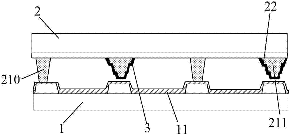
[0032] This embodiment provides an organic light emitting diode device, such as figure 1 As shown in the figure, it includes a first substrate 1 and a second substrate 2 that are arranged opposite to each other, a first electrode 11 is provided on the side of the first substrate 1 close to the second substrate 2, and the second substrate 2 is close to the first substrate One side of 1 is provided with a first spacer 211 , wherein, the outer surface of the first spacer 211 close to the first substrate 1 has an uneven structure 22 , and the first spacer 211 is close to the outer surface of the first substrate 1 . The surface is covered with an auxiliary electrode layer 3 , and at least a part of the auxiliary electrode layer 3 is connected to the first electrode 11 . It should be noted that the auxiliary electrode layer may partially or completely cover the outer surface of the first spacer, as long as it is ensured that the auxiliary electrode layer is in contact with the first...

Embodiment 2

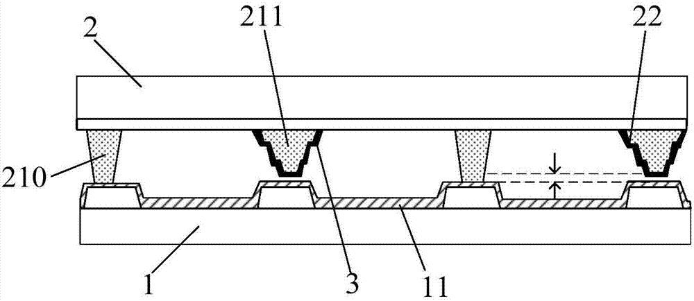
[0035] This embodiment provides an organic light emitting diode device, such as figure 2 As shown in the figure, it includes a first substrate 1 and a second substrate 2 that are oppositely arranged. A first electrode 11 is provided above the surface of the first substrate 1 close to the second substrate 2, and the second substrate 2 is close to the first substrate. 1 is provided with a main spacer 210 and a first spacer 211 ; the surface of the first spacer 211 close to the first substrate 1 has an uneven structure 22 , and the uneven structure 22 is close to the surface of the first substrate 1 . One side is covered with an auxiliary electrode layer 3 , and at least part of the auxiliary electrode layer 3 is connected to the first electrode 11 .

[0036] Among them, see Figure 5 , the uneven structure 22 of this embodiment includes but is not limited to Figure 5 The irregular surface a, the arc surface b, the rhomboid surface c, and the uneven surface d shown in the cro...

Embodiment 3

[0059] This embodiment provides a method for fabricating an organic light emitting diode device. The organic light emitting diode device in this embodiment includes a first substrate 1 and a second substrate 2. The first substrate 1 and the second substrate 2 are separately prepared and then packaged in a box. Specifically include the following steps:

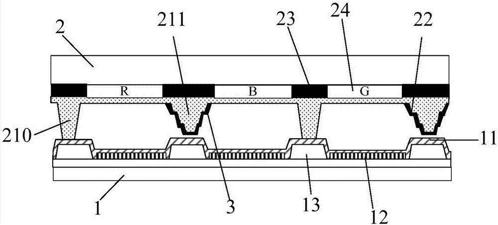
[0060] S01 , forming a first electrode 11 on the first substrate 1 ; wherein, the structure on the first substrate 1 further includes a driving circuit layer, a pixel defining structure layer 13 and a light-emitting functional layer 12 . The preparation method of S01 is as follows:

[0061] S01a, cleaning the substrate of the first substrate 1; then preparing the TFT process of the driving circuit layer on the substrate of the first substrate 1;

[0062] S01b, coating a layer of photocurable material with a thickness of 1.6-2.0 microns by spin coating, and after pre-baking, exposing, developing, and post-baking, and patterning...


PUM


Abstract

The invention provides an organic light emitting diode device, a manufacturing method thereof and a display device, and belongs to the technical field of display. The problem that an existing top-emitting AMOLED cathode material is poor in light transmittance or conductivity can be solved. A first spacer on a second substrate in the organic light emitting diode device has an uneven structure, so that adhesion of an auxiliary electrode material is facilitated; the height of the first spacer is different from that of a main spacer, wherein the high spacer mainly plays a role in supporting, and when the device bears pressure, the high spacer can achieve supporting and pressure buffering functions so that an auxiliary electrode on the first spacer can be protected when making contact with a first electrode on a first substrate, the auxiliary electrode is prevented from being broken, and the conductivity of the whole first electrode is enhanced. The organic light-emitting diode device is suitable for various display devices.

Description

technical field [0001] The invention belongs to the technical field of display, and in particular relates to an organic light-emitting diode device, a preparation method thereof, and a display device. Background technique [0002] At present, organic light emitting diode (Organic Light Emitting Diode, OLED) devices are developing rapidly in the field of flat panel display with the characteristics of thinness, low consumption, high response, and high resolution, and their potential market prospects are favored by the industry. [0003] Top emission passive organic light emitting diodes (Active-matrix organic light emitting diodes, AMOLEDs) can effectively solve the problems of reduced aperture ratio and display brightness caused by complex TFT (thin film field effect transistor) compensation circuits. The microcavity effect existing in the structure of the top emission AMOLED device can also improve the color gamut of the AMOLED display screen and improve the display effect. ...

Claims


Application Information

Patent Timeline
Patent Type & Authority Applications(China)
IPC IPC(8): H01L51/50H01L51/52H01L27/32
CPCH10K59/00H10K50/00H10K50/80H10K50/805H10K59/38H10K59/1315H10K50/8428H10K50/865H10K59/122H10K50/81H10K50/131H10K50/824H10K59/126
Inventor 李伟张星谢蒂旎
Owner BOE TECH GRP CO LTD
Why Eureka
Try Eureka