Semiconductor device and manufacturing method thereof

A manufacturing method and semiconductor technology, which are applied in the fields of semiconductor devices, semiconductor/solid-state device manufacturing, electric solid-state devices, etc., can solve the problem that the cathode and the auxiliary cathode cannot be well overlapped, so as to avoid uneven light emission, reduce the width, and improve the The effect of stability

Pending Publication Date: 2021-02-05
FUJIAN HUAJIACAI CO LTD
View PDF1 Cites 0 Cited by
  • Summary
  • Abstract
  • Description
  • Claims
  • Application Information

AI Technical Summary

Problems solved by technology

[0005] Therefore, it is necessary to provide a semiconductor device and a manufacturing method to solve the problem that the cathode and the auxiliary cathode cannot be well bonded together

Method used


Image

  • Semiconductor device and manufacturing method thereof
  • Semiconductor device and manufacturing method thereof
  • Semiconductor device and manufacturing method thereof

Examples


Embodiment Construction

[0051] In order to explain in detail the technical content, structural features, achieved goals and effects of the technical solution, the following will be described in detail in conjunction with specific embodiments and accompanying drawings.

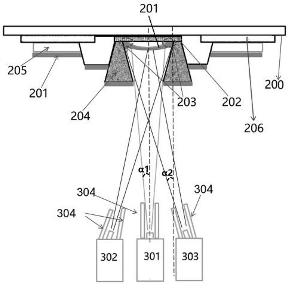
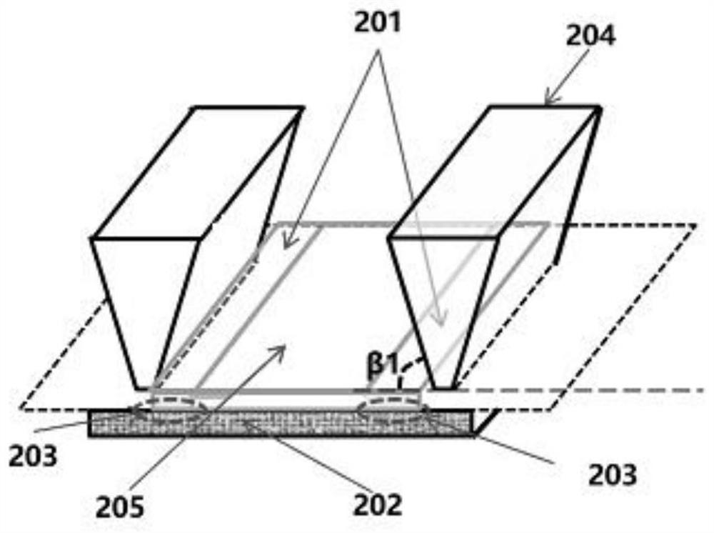
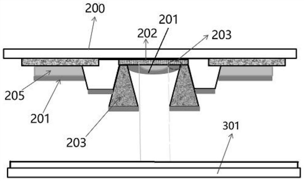
[0052] see Figure 1 to Figure 4 , the present embodiment provides a method for manufacturing a semiconductor device, including the following steps: making an auxiliary cathode 202 on a substrate 200; specifically, coating a layer of photoresist on the substrate 200, patterning the photoresist, that is, exposing and developing the photoresist , so that the part where the auxiliary cathode 202 is to be made is opened. The auxiliary cathode material is plated by evaporation to form an auxiliary cathode 202 on the substrate 200, with a structure such as figure 1 shown. Wherein, the auxiliary cathode material may be one or more metals among Al (aluminum), Ag (silver), and Au (gold). The thickness of the auxiliary cathode 202 is 1 um (m...


PUM


Abstract

The invention provides a semiconductor device and a manufacturing method thereof. The manufacturing method comprises the following steps: manufacturing an auxiliary cathode on a substrate; manufacturing an isolation layer with a slot, wherein the bottom width of the slot is greater than the top width of the slot; forming an organic film layer on the substrate through a first evaporation source, and when steam of the first evaporation source passes through the open groove, enabling the part, not shielded by the top of the open groove, of the steam to enter the bottom of the open groove to formthe organic film layer; forming a gap between the side edge of the organic film layer and the side edge of the bottom of the slot, and exposing the auxiliary cathode; and forming a cathode on the substrate in an evaporation mode, enabling steam in the evaporation process to penetrate through the top of the open groove from different angles and cover the whole bottom of the open groove, enabling the cathode to cover the organic film layer in the open groove, and connecting the side edge of the cathode with the auxiliary cathode through the gap. According to the technical scheme, the stability of the cathode in the working process can be improved, and the phenomenon of uneven light emitting (IR-Drop phenomenon) of a semiconductor device (such as a display panel) is avoided.

Description

technical field [0001] The invention relates to the field of semiconductor manufacturing, in particular to a semiconductor device and a manufacturing method. Background technique [0002] Organic light-emitting diode (Organic Light-Emitting Diode, abbreviated as OLED) device has been widely used in the display field due to its advantages of self-luminescence, thinness, fast response speed and easy realization of flexibility, and it is currently the most promising display technology. [0003] The light-emitting part of an OLED device is mainly composed of a cathode, an anode and an organic layer sandwiched between them. When preparing an OLED device, an organic film layer is first evaporated on a substrate prepared with an anode, and then a cathode is evaporated. When the OLED device is working, current is injected from the electrode to the organic layer to form excitons and emit light. The anode of the OLED device is generally composed of a metal film layer or ITO, and th...

Claims


Application Information

Patent Timeline
Patent Type & Authority Applications(China)
IPC IPC(8): H01L51/52H01L51/56H01L27/32G02F1/1343
CPCG02F1/134309H10K59/10H10K50/824H10K50/844H10K71/00
Inventor 乔小平
Owner FUJIAN HUAJIACAI CO LTD
Why Eureka
Try Eureka