Alignment operation process of overlay process in PDMS micro-fluidic chip processing

A microfluidic chip and operation process technology, which is applied in the field of overlay lithography operation process, can solve the problems of increasing the difficulty of alignment operation, and achieve the effect of reducing the difficulty of rough alignment, reducing repeated searching, and reducing difficulty

Active Publication Date: 2021-02-09
NANTONG UNIVERSITY
View PDF3 Cites 0 Cited by
  • Summary
  • Abstract
  • Description
  • Claims
  • Application Information

AI Technical Summary

Problems solved by technology

In addition, the movement direction of objects under the microscope eyepiece is inconsistent with our cognitive habits, which also increases the difficulty of alignment operations. We look forward to the development of optimized and systematic alignment processes

Method used


Image

  • Alignment operation process of overlay process in PDMS micro-fluidic chip processing
  • Alignment operation process of overlay process in PDMS micro-fluidic chip processing
  • Alignment operation process of overlay process in PDMS micro-fluidic chip processing

Examples


Embodiment

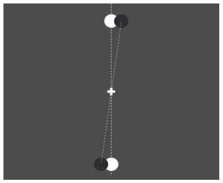
[0023] Overlaying is a highly difficult operation in the photolithography process. The overlaying process of microfluidic chips with high precision requirements requires experienced operators to perform, and it takes a whole hour to process and produce microfluidic chips with high overlay accuracy. , need to be repeatedly debugged on the lithography machine.

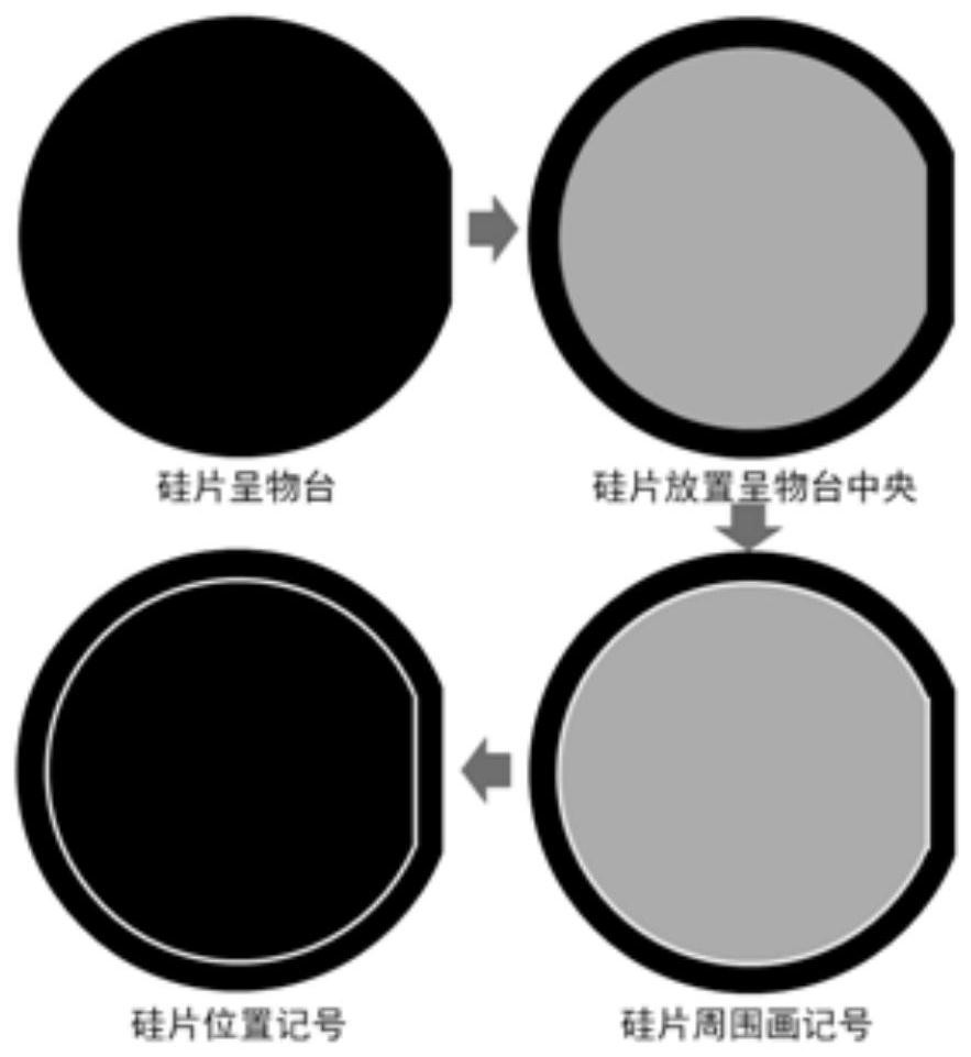
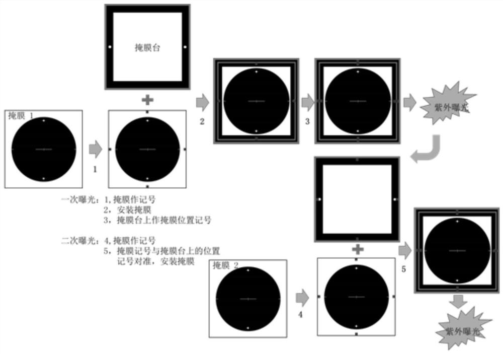
[0024]When designing the microfluidic chip manufacturing and processing mask, the alignment marks of the mask used for the first exposure and the mask for the second exposure are designed at the same position of the mask. In this way, as long as the second exposure during the first exposure and overlay The installation positions of the two masks on the mask table are exactly the same, and the alignment can be achieved by ensuring that the front and rear silicon wafers are also placed in the same position. This design can be called "position overlapping" mask silicon wafer installation, which can The mask alignment mark i...


PUM


Abstract

The invention discloses an alignment operation process of an overlay process in PDMS micro-fluidic chip processing, which fully and systematically prepares before photoetching, is handy during photoetching, and can quickly and smoothly complete overlay alignment. After the preparation work is finished, the operation time of the photoetching machine can be controlled within half an hour, so that the working efficiency is improved, and the consumption of the machine is reduced. By the adoption of the technical scheme, a beginner can well complete high-difficulty overlay alignment. By using the technical scheme, the alignment result which is the same as that of an imported photoetching machine ABM.Inc.Mask Aligner can also be realized when an ordinary domestic exposure machine JKG-2A is usedfor alignment, the alignment deviation is less than 5 microns when the technology is used for alignment of microfluidic processing, but the alignment precision is required as long as a high channel and a low channel can be communicated, and the processing and use requirements of microfluidic chips are completely met.

Description

technical field [0001] The invention relates to an operation process flow of overlay photolithography, in particular to an alignment process flow of overlay alignment exposure in processing and manufacturing PDMS microfluidic chips. Background technique [0002] UV lithography is a commonly used technology in the field of micro-nano processing, for example, it is used in integrated circuit manufacturing, micro-optics, micro-mechanics and the rapid development of microfluidic chip processing in recent years. Another example is that Huawei's mobile phone manufacturing, which has attracted more attention recently, is limited by the supply of chips. The bottleneck restricting chip manufacturing is photolithography. The photolithography process is to transfer the pattern on the mask to the photoresist coated on the surface of the silicon wafer (silicon wafer) through exposure technology, and then transfer the pattern to the silicon wafer through processes such as development, har...

Claims


Application Information

Patent Timeline
IPC IPC(8): G03F9/00
CPCG03F9/7023
Inventor 赵幸福孙逸凡印唐臣朱海燕张迎洁
Owner NANTONG UNIVERSITY
Why Eureka
Try Eureka