High-frequency anti-reverse silicon stack and high-frequency boosting transformer

A step-up transformer and transformer technology, applied in the field of transformers, can solve the problems of poor space utilization, human injury, low voltage withstand level, etc., and achieve the effect of compact arrangement structure, reducing human injury, and increasing insulation voltage

Active Publication Date: 2021-02-09
XJ POWER CO LTD
View PDF6 Cites 0 Cited by
  • Summary
  • Abstract
  • Description
  • Claims
  • Application Information

AI Technical Summary

Problems solved by technology

[0002] At present, high-power high-voltage step-up transformers and high-frequency rectification circuits mostly use transformer secondary winding in segments, and then multi-stage cascading. Since ordinary silicon stacks are easily damaged, high-frequency rectification in the prior art uses high-voltage and high-frequency silicon stacks. rectified output
Although this method can reduce the influence of the inter-turn distributed capacitance of the secondary winding on the high-frequency rectification circuit, the high-voltage and high-frequency rectifier silicon stack used as a rectifier device is relatively large and cannot meet the rectification of AC power above 200kHz. During the structural design process of high-power high-voltage step-up transformers and high-frequency rectifier circuits, the space utilization rate is poor, resulting in that the discharge devices in the prior art are generally placed outside the transformer, and there is no discharge circuit inside the transformer, and the high-voltage electric energy stored inside It is easy to cause harm to the human body, and the withstand voltage level is low

Method used


Image

  • High-frequency anti-reverse silicon stack and high-frequency boosting transformer
  • High-frequency anti-reverse silicon stack and high-frequency boosting transformer
  • High-frequency anti-reverse silicon stack and high-frequency boosting transformer

Examples


Embodiment Construction

[0037] In order to make the purpose, technical solutions and advantages of the embodiments of the present invention clearer, the technical solutions in the embodiments of the present invention will be clearly and completely described below in conjunction with the drawings in the embodiments of the present invention. Obviously, the described embodiments It is a part of embodiments of the present invention, but not all embodiments. The components of the embodiments of the invention generally described and illustrated in the figures herein can be arranged and designed in a variety of different configurations.

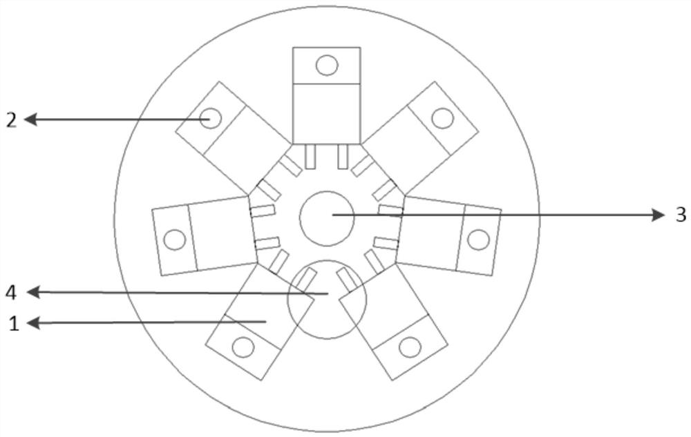
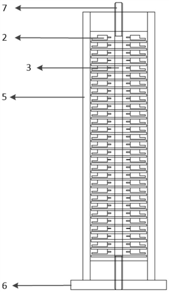
[0038] Please refer to Figure 1 to Figure 2 , The first embodiment of the present invention provides a high-frequency anti-reflection silicon stack, including an insulating cover 5, and the high-frequency diodes 1 are stacked and installed in the insulating cover 5 through a combined support member.

[0039] The composite support is formed by connecting several layers of...


PUM


Abstract

The invention discloses a high-frequency anti-reverse silicon stack and a high-frequency boosting transformer. The high-frequency anti-reverse silicon stack comprises an insulating cover, and high-frequency diodes are stacked and installed in the insulating cover through combined supporting pieces. The combined supporting pieces are formed by connecting a plurality of layers of supporting pieces from top to bottom, and an inner fixing hole is formed in the center of each layer of supporting pieces and is used for fixing the inner side of each high-frequency diode; a plurality of outer fixing holes are formed in each layer of supporting pieces along the same radius and are used for fixing the outer side of each high-frequency diode; and a preformed hole is formed between every two adjacentlayers of supporting pieces so as to fix the last high-frequency diode of the upper layer and the first high-frequency diode of the lower layer. The high-frequency boosting transformer comprises a high-voltage output aviation plug, a transformer primary coil, a transformer secondary coil, a discharge loop, a high-frequency rectifying plate, a discharge resistor and the high-frequency anti-reversesilicon stack. The high-frequency anti-reverse silicon stack and the high-frequency boosting transformer are compact in structure and small in size, residual voltage can be discharged in time, and damage of the residual voltage to the human body is reduced.

Description

technical field [0001] The invention relates to the technical field of transformers, in particular to a high-frequency anti-anti-silicon stack and a high-frequency step-up transformer. Background technique [0002] At present, high-power high-voltage step-up transformers and high-frequency rectification circuits mostly use transformer secondary winding in segments, and then multi-stage cascading. Since ordinary silicon stacks are easily damaged, high-frequency rectification in the prior art uses high-voltage and high-frequency silicon stacks. Perform rectified output. Although this method can reduce the influence of the inter-turn distributed capacitance of the secondary winding on the high-frequency rectification circuit, the high-voltage and high-frequency rectifier silicon stack used as a rectifier device is relatively large and cannot meet the rectification of AC power above 200kHz. During the structural design process of high-power high-voltage step-up transformers and...

Claims


Application Information

Patent Timeline
Patent Type & Authority Applications(China)
IPC IPC(8): H02M7/00H02M7/08H01F27/40
CPCH02M7/003H02M7/08H01F27/40
Inventor 张向炜袁攀夏德印田勤皇利杰李振国赵莹莹牛智莉李海燕陈丽陈璐明冯进喜李鹏军宁文斌宋军伟韩大鹏
Owner XJ POWER CO LTD
Why Eureka
Try Eureka