
A kind of manufacturing process of solar p-type polysilicon wafer

A polycrystalline silicon wafer and manufacturing process technology, applied in manufacturing tools, polycrystalline material growth, fine working devices, etc., can solve problems such as light-induced attenuation, achieve fast heating speed, uniform heating, and more consistent grain growth Effect

Active Publication Date: 2022-02-08
ANYANG INST OF TECH
View PDF0 Cites 0 Cited by
  • Summary
  • Abstract
  • Description
  • Claims
  • Application Information

AI Technical Summary

Problems solved by technology

Due to the presence of B-O complexes in solar cells prepared by B-doped P-type silicon wafers, which leads to light-induced attenuation, the dopant of P-type silicon wafers is gradually replaced by Ga elements from traditional B elements.

Method used


Image

  • A kind of manufacturing process of solar p-type polysilicon wafer
  • A kind of manufacturing process of solar p-type polysilicon wafer
  • A kind of manufacturing process of solar p-type polysilicon wafer

Examples


preparation example Construction

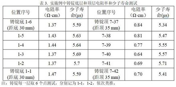
[0028] Preparation of P-type silicon ingot: In an argon atmosphere, the silicon material was sintered to 1550 °C in a microwave sintering furnace, and the microwave frequency was 2.45 GHz ± 25 MHz. The heating rate was 26 ℃ / min, and the heat preservation was 120 min. The whole process of temperature rise and fall was protected and cooled by argon gas, and the purity of argon gas was 4 N (99.99%). The role of argon is to prevent the silicon material from being oxidized during the heating process. The temperature of the microwave sintering furnace is controlled by an intelligent control system, and the temperature is measured by infrared rays. The microwave generated by the microwave sintering furnace is diffracted (diffraction) inside the silicon material, and the silicon material is heated at the same time, with a fast heating rate and less heat loss. Compared with a resistance furnace, the same temperature increase can save energy by more than 40%. At the same time, the sil...

Embodiment

[0040] Step 1: Prepare P-type recycled silicon material. The recycled silicon material contains metal impurities such as hair, staples, and diamond wires, and organic impurities such as sticky glue, sticky board glue, and resin board. After magnetic separation, hot water degumming, carbonization and other stages, and then after 20% HF corrosion, 25% HCl and 30% H 2 o 2 Mixed liquid pickling, water isolation, 12% NaOH alkali washing and other stages, followed by appropriate concentration of HCl to neutralize the residual liquid on the surface of the fragments, deionized water ultrasonic rinsing and other procedures, the final rinse water conductivity 936 μS / cm, Rinse water pH = 7.01. After drying in a microwave oven at 105 ℃, manual sorting and other procedures, the broken silicon wafers without impurities are packaged and put into storage. Manual sorting mainly screens non-silicon impurities such as stones that cannot be treated by pickling, alkali washing and other procedu...


PUM

PropertyMeasurementUnit
purityaaaaaaaaaa
heightaaaaaaaaaa
electrical resistivityaaaaaaaaaa

Abstract

The invention discloses a manufacturing process of solar P-type polycrystalline silicon wafers. The production process steps include: (1) preparation of raw materials; (2) preparation of P-type silicon ingots; (3) cutting and prescribing of silicon ingots; (4) silicon ingots Cutting and cleaning of slices; the raw materials used include: primary silicon material with a purity of 6N, recycled silicon material, and dopant gallium; the recycled silicon material includes recycled silicon plates, recycled silicon blocks, recycled silicon wafers, and recycled silicon powder. The recycled silicon material needs to be purified before use. The edge of the crucible is filled with recycled silicon material when the ingot is cast, and the center of the crucible is filled with gallium-doped primary silicon material. The doping concentration of gallium in the primary silicon material is from From the bottom of the crucible to the top of the crucible gradually decreases, the concentration of gallium at the top is zero, and then the crucible filled with silicon material is placed in a microwave sintering furnace. P-type silicon ingots. The invention fully utilizes the recycled silicon material, and the quality of the prepared silicon chips is stable.

Description

technical field [0001] The invention specifically relates to a manufacturing process of a solar P-type polysilicon wafer, which belongs to the technical field of semiconductor materials. Background technique [0002] The photoelectric conversion efficiency of solar cells is closely related to the quality of solar silicon wafers, and the purity of silicon wafers is generally required to be no less than 6N (99.9999%). The manufacturing process of polysilicon wafers usually includes ingot casting, squaring, slicing, testing and packaging, etc. During this process, a large amount of recycled silicon materials will be produced, including ① the top skin, bottom skin and side skin cut off during the cutting process of the silicon ingot etc., generally in the shape of a thin plate (circular silicon plate, silicon block), the content of impurity elements in these parts is higher than that of primary silicon; ② Incomplete and damaged single crystal silicon wafers or polycrystalline si...

Claims


Application Information

Patent Timeline
Patent Type & Authority Patents(China)
IPC IPC(8): C30B28/04C30B29/06B28D5/00
CPCC30B28/04C30B29/06B28D5/00
Inventor 刘振东刘笑笑晁军峰
Owner ANYANG INST OF TECH
Learn More