
Low-frequency low-power-consumption array substrate and manufacturing method thereof

A technology for array substrates and manufacturing methods, which is applied in the field of low-frequency and low-power array substrates and their manufacture, can solve problems such as space occupation, pixel density reduction, and liquid crystal panel resolution reduction, and achieve the effect of reducing area and ensuring pixel resolution

Inactive Publication Date: 2021-02-12
信利(仁寿)高端显示科技有限公司
View PDF8 Cites 2 Cited by
  • Summary
  • Abstract
  • Description
  • Claims
  • Application Information

AI Technical Summary

Problems solved by technology

After the refresh frequency is reduced, in order not to affect the display effect of the liquid crystal panel, the voltage sustaining time of the pixel electrode needs to be increased, that is to say, the area of ​​the storage capacitor needs to be increased to store more charge each time, but the The increase in the area of ​​the storage capacitor will occupy the space of the pixel electrode, so that the pixel density will be reduced, and the resolution of the liquid crystal panel will be reduced.

Method used


Image

  • Low-frequency low-power-consumption array substrate and manufacturing method thereof
  • Low-frequency low-power-consumption array substrate and manufacturing method thereof
  • Low-frequency low-power-consumption array substrate and manufacturing method thereof

Examples


Embodiment Construction

[0046] The present invention will be described in detail below in conjunction with the accompanying drawings and embodiments.

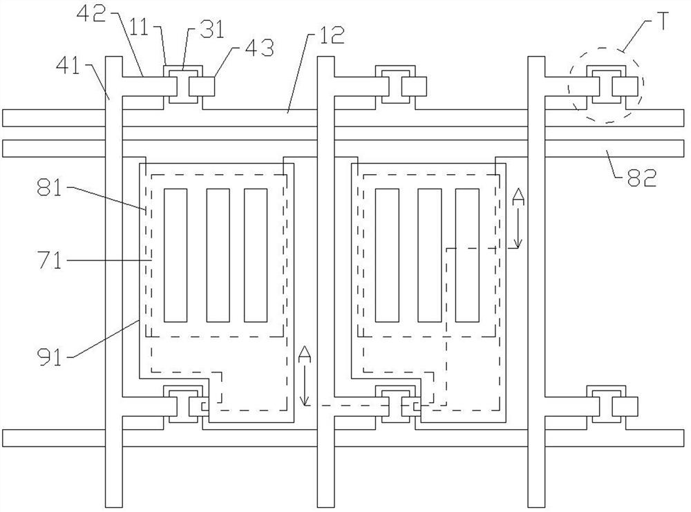
[0047] Such as Figure 1-6 As shown, a low-frequency and low-power array substrate includes a switch area and a pixel area.

[0048] The switch region includes a thin film transistor T, and the thin film transistor T includes a gate layer stacked up and down, a gate insulating layer 2, an active layer, a source drain layer, a first insulating layer 5 and a second insulating layer 6, and the gate The layer includes a gate 11 and a gate line 12 (GATE), the gate 11 is electrically connected to the gate line 12; the active layer includes a silicon island 31 on the gate insulating layer 2, the The silicon island 31 overlaps with the gate 11; the source-drain layer includes a data line 41 (SD) on the gate insulating layer 2, a source 42 on one side of the silicon island 31, a The drain 43 on the other side of the silicon island 31 is electrically connecte...


PUM


Abstract

The invention discloses a low-frequency low-power-consumption array substrate which comprises a pixel area; the pixel area comprises a first electrode layer, a first insulating layer, a second electrode layer, a second insulating layer and a third electrode layer which are stacked up and down, the first electrode layer comprises a first electrode, and the second electrode layer comprises a secondelectrode; the third electrode layer comprises a third electrode; the first electrode and the second electrode are at least partially overlapped up and down, so that a first storage capacitor is formed by the upper and lower overlapped parts of the first electrode and the second electrode; and the second electrode and the third electrode are at least partially overlapped up and down, so that a second storage capacitor is formed by the upper and lower overlapped parts of the second electrode and the third electrode. According to the low-frequency low-power-consumption array substrate, the voltage maintaining time of the pixel electrode can be prolonged under the condition that the resolution is not reduced, so that the pixel electrode still has sufficient voltage maintaining time in a low-frequency and low-power-consumption working state. The invention further discloses a manufacturing method of the low-frequency low-power-consumption array substrate.

Description

technical field [0001] The invention relates to display technology, in particular to a low-frequency and low-power consumption array substrate and a manufacturing method thereof. Background technique [0002] With the development of the panel display industry, the resolution requirements of the liquid crystal panel are getting higher and higher, and the power consumption of the liquid crystal panel is also increasing accordingly. In order to reduce power consumption without lowering the resolution, it is often used to reduce the refresh frequency of the liquid crystal panel to achieve the purpose of reducing power consumption. [0003] In the prior art, a common electrode layer VCOM is provided on the TFT substrate of the liquid crystal panel, and the common electrode in the common electrode layer VCOM will insulate and overlap with the pixel electrodes to form a storage capacitor. The liquid crystal panel relies on the The storage capacitor is used so that the pixel electr...

Claims


Application Information

Patent Timeline
Patent Type & Authority Applications(China)
IPC IPC(8): G02F1/1343G02F1/1362H01L27/12H01L21/84
CPCG02F1/134309G02F1/136213G02F1/136286G02F1/136227H01L27/124H01L27/1255H01L27/1259
Inventor 董欣于靖张东琪张泽鹏伍小丰
Owner 信利(仁寿)高端显示科技有限公司
Learn More