Semiconductor transistor die bonding auxiliary equipment

A technology for auxiliary equipment and transistors, which is used in semiconductor/solid-state device manufacturing, cleaning methods using gas flow, electrical components, etc., and can solve problems affecting patch accuracy and transistor transfer belt displacement

Inactive Publication Date: 2021-02-12
汪玉婷
View PDF0 Cites 0 Cited by
  • Summary
  • Abstract
  • Description
  • Claims
  • Application Information

AI Technical Summary

Problems solved by technology

[0004] Aiming at the deficiencies in the prior art, the object of the present invention is to provide an auxiliary device for bonding semiconductor transistors to solve the problem of placing the transistor on It is passed on the conveyor belt, and in the process of placement, the transmission of the transistor has a certain inertia, and the placement head exerts a downward pressure on it at the moment of placement, causing the transistor to be displaced on the conveyor belt to a certain extent, resulting in the advance. A good patch head will stick the patch to the wrong side, which will affect the accuracy of the subsequent patch

Method used


Image

  • Semiconductor transistor die bonding auxiliary equipment
  • Semiconductor transistor die bonding auxiliary equipment
  • Semiconductor transistor die bonding auxiliary equipment

Examples


Embodiment 1

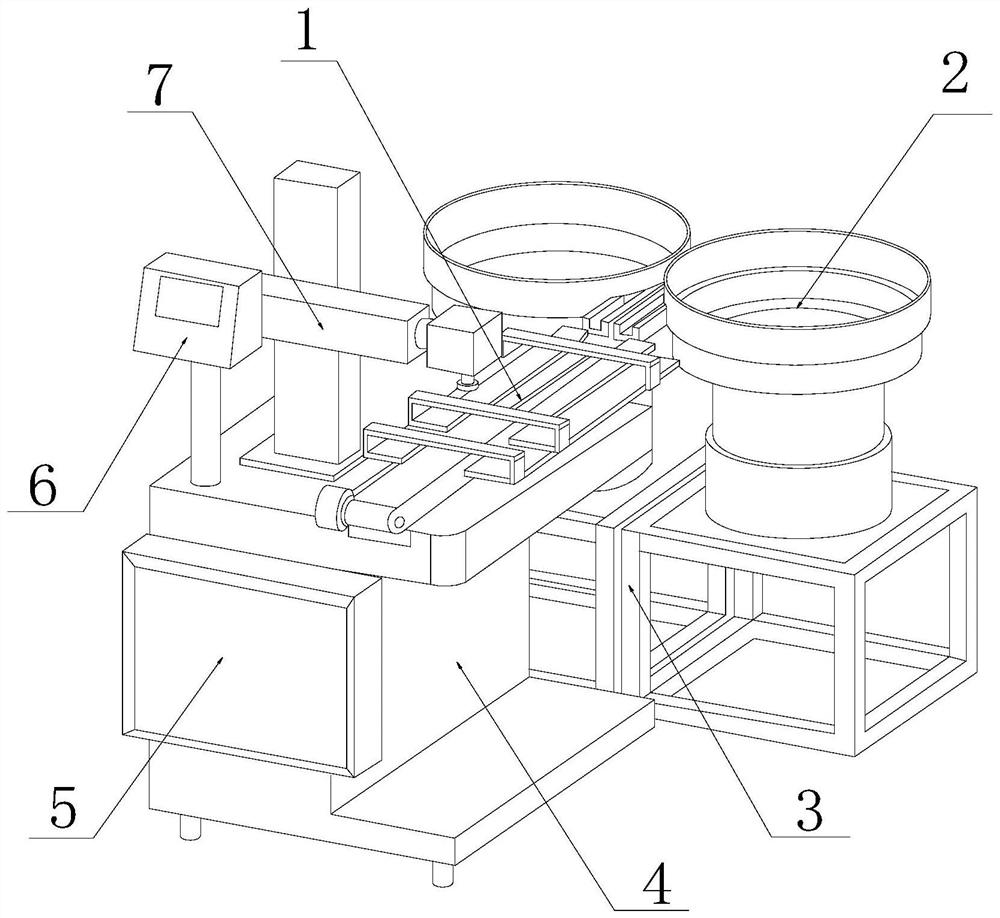
[0026] as attached figure 1 to attach Figure 5 Shown:

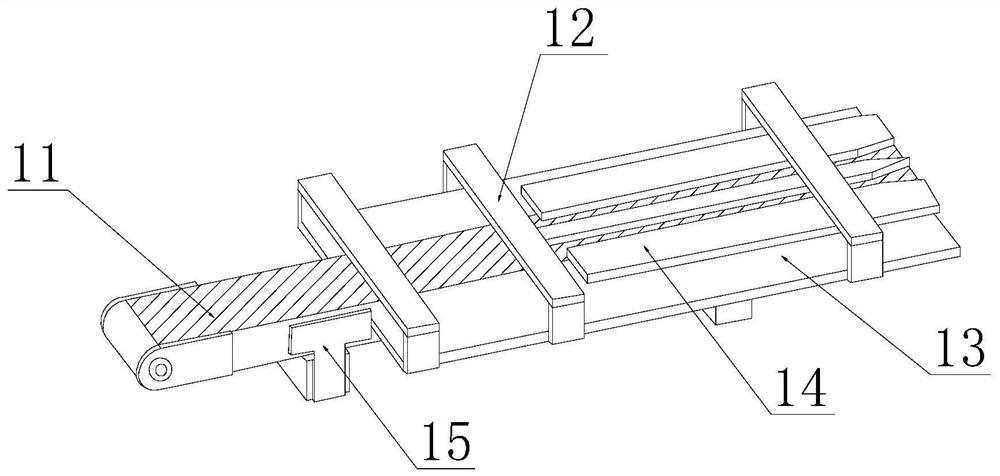
[0027] Its structure includes a conveyor 1, a feeding trough 2, a support platform 3, a carrier platform 4, an equipment box 5, a controller 6, and a film sticking head 7. 3 is fixed with bolts at the bottom of the lower chute 2, the carrier platform 4 is in clearance fit with the left side of the support platform 3, the carrier platform 4 is movably matched with both sides of the conveyor 1, and the carrier platform 4 is matched with the left side of the equipment box 5 Embedded connection, the controller 6 is fixed on the upper surface of the carrier 4 and nested with it, the adhesive head 7 is bolted to the upper surface of the carrier 4, the conveyor 1 is movably matched with the top of the adhesive head 7, the The conveyor 1 includes a conveyor belt 11, an air supply frame 12, a fixed plate 13, a limit block 14, and a support seat 15. The center is nested and connected, the surface of the fixed plate 13 is bolted...

Embodiment 2

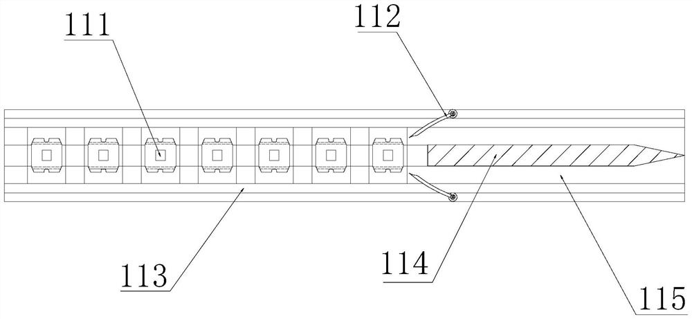
[0034] as attached Image 6 to attach Figure 7 Shown:

[0035] Wherein, the air supply frame 12 includes a support frame 121, an air duct 122, and an air outlet column 123, the bottom surface of the support frame 121 is integrally connected with the air duct 122 by bolts, and the surface of the air duct 122 cooperates with the inside of the air outlet column 123. , the support frame 121 is connected with bolts at the top of the air outlet column 123, and the air outlet column 123 is provided with three elliptical cylinders, which are small at the top and large at the bottom, distributed on the lower surface of the support frame 121, and fixed with the bolts, wherein The column 123 is beneficial to cooperate with the air duct 122 to blow off the dust and debris on the surface of the transistor and the surroundings, so as to ensure that there will be no problem of sticking or not sticking the chips when bonding the chips.

[0036] Wherein, the air outlet column 123 includes a...


PUM


Abstract

The invention discloses semiconductor transistor die bonding auxiliary equipment, and the equipment structurally comprises a conveyor, a discharging groove, a support table, a carrying table, an equipment box, a controller and a die bonding head. The right end of the conveyor is movably matched with the discharging groove, the support table is fixed to the bottom end of the discharging groove through bolts, the carrying table is in clearance fit with the left side of the support table, and the carrying table is movably matched with the two sides of the conveyor; the carrying table is fixedly connected with the left side of the equipment box in an embedded mode, the controller is fixed to the upper surface of the carrying table and connected with the carrying table in an embedded mode, thedie bonding head is connected with a bolt on the upper surface of the carrying table, and the conveyor is movably matched with the top end of the die bonding head. The conveyor comprises a conveying belt, an air supply frame, a fixed plate, a limiting block and a supporting base. A transistor needing chip mounting is effectively fixed through the storage groove in the conveying belt, it is guaranteed that when the chip mounting head carries out chip mounting, the phenomenon that displacement is generated due to the downward pressure of the chip mounting head, and consequently chip mounting dislocation is caused is avoided, and the problem that the chip mounting head which is aligned in advance pastes a chip obliquely, and consequently the precision of subsequent chip mounting is affected is effectively solved.

Description

technical field [0001] The invention relates to the field of transistors, in particular to an auxiliary device for bonding semiconductor transistors. Background technique [0002] Transistors are also called semiconductor transistors. Semiconductors are a kind of material whose conductivity is between conductors and insulators. At present, most of the materials used to make semiconductors are silicon and germanium. Because this substance has a crystal structure, it is called is a semiconductor transistor; [0003] However, there are the following deficiencies in the prior art: the existing semiconductor transistor chip bonding auxiliary equipment needs to place the transistor on the conveyor belt and transfer it in during the assembly process of the existing semiconductor transistor chip bonding process, and the transistor transmission has a certain inertia during the chip bonding process. , the placement head exerts a downward pressure on it at the moment of placement, cau...

Claims


Application Information

Patent Timeline
IPC IPC(8): H01L21/687B08B5/02
CPCB08B5/023H01L21/68721
Inventor 汪玉婷
Owner 汪玉婷
Why Eureka
Try Eureka