Groove type positioning method of 3D wafer

A positioning method and wafer technology, applied to electrical components, electrical solid devices, circuits, etc., can solve problems such as poor positioning and affecting production efficiency

Pending Publication Date: 2021-03-02
太极半导体(苏州)有限公司
View PDF0 Cites 2 Cited by
  • Summary
  • Abstract
  • Description
  • Claims
  • Application Information

AI Technical Summary

Problems solved by technology

[0002] The wafer needs to be positioned by the recognition sensor first during processing. The existing method is to make a small gap on the outer edge of the wafer. However, due to the current implement

Method used


Image

  • Groove type positioning method of 3D wafer

Examples


Embodiment Construction

[0014] The present invention is described below in conjunction with accompanying drawing.

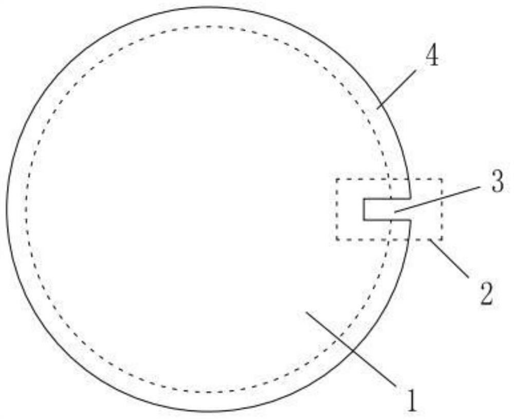
[0015] as attached figure 1 As shown, a slot-type positioning method for a 3D wafer according to the present invention includes a wafer 1 and a positioning sensor 2; a positioning slot 3 is first processed on the edge of the wafer 1, and the positioning slot 3 can be a rectangular slot. Or other elongated regular shapes, the center line of the rectangular groove along the long side passes through the center of the wafer 1; the positioning groove 3 is processed by laser or physical cutting, and the depth of the positioning groove 3 is 3-8mm, Wafer 1 is then ring-cut to remove abnormal parts of the thickness of the outer circle of wafer 1, and the difference between the outer diameter and inner diameter of the removed ring-cut part 4 is less than the depth of positioning groove 3; after wafer 1 is ring-cut, the outer There is still a part of the positioning groove 3 structure on the circ...


PUM

PropertyMeasurementUnit
Depthaaaaaaaaaa

Abstract

The invention discloses a groove type positioning method of a 3D wafer. A wafer and a positioning sensor are included. The method comprises the steps that a positioning groove is machined in the edgeof a wafer, then girdling is conducted on the wafer, the abnormal thickness part of the outer ring of the wafer is removed, and the difference between the outer diameter and the inner diameter of theremoved girdling part is smaller than the depth of the positioning groove; after the wafer is subjected to girdling, a part of positioning groove structure is still reserved on the outer ring; and thepositioning sensor is used for identifying the remaining positioning groove after the wafer is annularly cut so as to position the wafer; according to the scheme, the positioning groove is machined in the edge of the wafer and extends into the effective area of the wafer, possibility is provided for secondary machining of the edge of the 3D wafer, wafer positioning is not affected after the periphery of the 3D wafer is removed, the detectable inspection area is increased, and the positioning difficulty is reduced.

Description

technical field [0001] The invention relates to a slot-type positioning method for a 3D wafer, belonging to the technical field of semiconductor processing. Background technique [0002] The wafer needs to be positioned by the recognition sensor first during processing. The existing method is to make a small gap on the outer edge of the wafer. However, due to the current implementation of 3D wafers, the peripheral thickness of the wafer has changed, resulting in equipment Frequent "poor positioning" alarms occur during wafer positioning, seriously affecting production efficiency. Contents of the invention [0003] In view of the above-mentioned existing technical problems, the object of the present invention is to propose a slot-type positioning method for 3D wafers. [0004] The technical solution of the present invention is realized in the following way: a slot-type positioning method for a 3D wafer, comprising a wafer and a positioning sensor; first processing a positi...

Claims


Application Information

Patent Timeline
IPC IPC(8): H01L23/544H01L21/68
CPCH01L21/681H01L23/544H01L2223/54493
Inventor 李峰杨健张光明
Owner 太极半导体(苏州)有限公司
Why Eureka
Try Eureka