
Semiconductor wafer clamping equipment

A clamping device and semiconductor technology, applied in the manufacture of semiconductor/solid-state devices, pollution prevention methods, electrical components, etc., can solve the problems affecting the surface finish of the wafer, easy to pollute the front of the wafer, etc., to achieve compact structure and improve efficiency , the effect of reducing pollution

Active Publication Date: 2021-03-09
SICHUAN FINE ARTS INST
View PDF11 Cites 2 Cited by
  • Summary
  • Abstract
  • Description
  • Claims
  • Application Information

AI Technical Summary

Problems solved by technology

However, when the back is cleaned, the cleaning agent on the back can easily contaminate the front of the wafer, affecting the smoothness of the front of the wafer.

Method used


Image

  • Semiconductor wafer clamping equipment
  • Semiconductor wafer clamping equipment
  • Semiconductor wafer clamping equipment

Examples


Embodiment Construction

[0023] Embodiments of the present invention are described below through specific examples, and those skilled in the art can easily understand other advantages and effects of the present invention from the content described in this specification. The present invention can also be implemented or applied through other different specific implementation modes, and various modifications or changes can be made to the details in this specification based on different viewpoints and applications without departing from the spirit of the present invention. It should be noted that the diagrams provided in the following embodiments are only schematically illustrating the basic concept of the present invention, and the following embodiments and the features in the embodiments can be combined with each other in the case of no conflict.

[0024] Wherein, the accompanying drawings are for illustrative purposes only, and represent only schematic diagrams, rather than physical drawings, and should...


PUM


Abstract

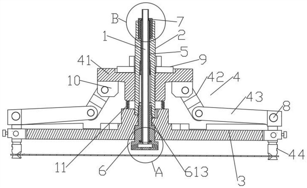
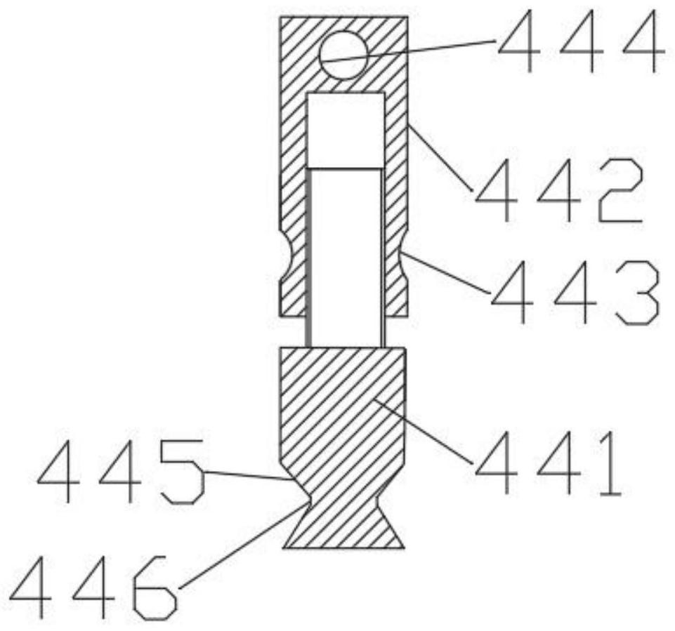
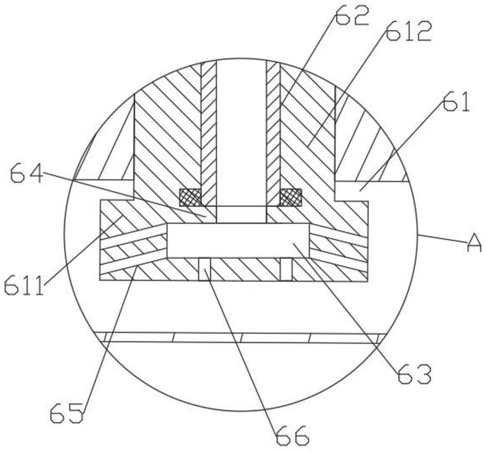
The invention discloses semiconductor wafer clamping equipment, and belongs to the technical field of semiconductors. The semiconductor wafer clamping equipment comprises a wafer clamping support anda gas ejector pipe rotationally arranged in the center of the wafer clamping bracket, wherein the wafer clamping support comprises a transmission connecting shaft, a support body fixedly arranged at the lower end of the transmission connecting shaft and a clamping finger assembly connected with the support body and used for clamping a wafer, the transmission connecting shaft is connected to a driving device, center holes used for being in running fit with the gas ejector pipe are formed in the center of the transmission connecting shaft and the center of the support body, and the lower end ofthe gas ejector pipe extends to the center of the side of the front face of the wafer. The device can be used for clamping the wafer when the back of the wafer is cleaned, and pollution to the front surface of the wafer is reduced while the wafer is stably cleaned.

Description

technical field [0001] The invention belongs to the technical field of semiconductors, and in particular relates to a semiconductor wafer clamping device. Background technique [0002] In the process of wafer processing, due to the use of a large number of new materials, the back of the wafer often has particle contamination, and the particle size can generally reach the order of microns. When the wafer is sent to the lithography machine, it is easy to form "bad spots" during exposure. ”, Therefore, the wafer needs to be cleaned on the back side when performing the next step of the process. However, when the back is cleaned, the cleaning agent on the back is very easy to contaminate the front of the wafer, affecting the smoothness of the front of the wafer, which is not worth the candle. Therefore, continue to provide a semiconductor wafer clamping device, which can be used for clamping the wafer during back cleaning, and can reduce the pollution on the front of the wafer w...

Claims


Application Information

Patent Timeline
Patent Type & Authority Applications(China)
IPC IPC(8): B08B17/02B08B13/00H01L21/687H01L21/67
CPCB08B17/02B08B13/00H01L21/68714H01L21/67017
Inventor 许娜
Owner SICHUAN FINE ARTS INST
Learn More