Coupling method of PLC optical branching device

A technology of optical splitter and optical waveguide, which is applied in the field of integrated optics, can solve the problems of increased chip R&D cost and R&D time, increased difficulty of chip design, and low production efficiency, so as to improve yield rate, optical performance, and R&D time Short, consistent effect

Active Publication Date: 2021-03-09
常州光芯集成光学有限公司
View PDF4 Cites 0 Cited by
  • Summary
  • Abstract
  • Description
  • Claims
  • Application Information

AI Technical Summary

Problems solved by technology

The chip design of the integrated planar waveguide optical splitter needs to consider the design tolerance and process debugging. With the increase of branches, the difficulty of chip design increases, and it is difficult to ensure that the limited number of designs and wafer tape-out results meet product requirements. R&D costs and R&D time are rising exponentially
On the other hand, using the conventional optical splitter coupling method to couple multiple input and multiple output optical splitters, the coupling method is complicated and the production efficiency is not high

Method used


Image

  • Coupling method of PLC optical branching device
  • Coupling method of PLC optical branching device
  • Coupling method of PLC optical branching device

Examples


Embodiment 1

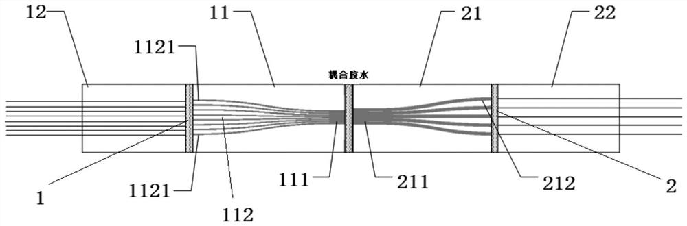
[0034] A coupling method for a PLC optical splitter, first coupling and bonding an optical splitter chip containing 1×2 with a 2-channel FA to form a 1×2 input component, and then combining an optical splitter chip containing 1×8 The chip is coupled with the 8-channel FA to form a 1×8 output component, and then the 1×2 input component and the 1×8 output component are collimated, coupled and bonded to each other to form a 2×8 optical splitter.

[0035] Among them, the width of the optical waveguide at the input end of the 1×2 optical splitter chip is 100 μm, and the width of the two optical waveguides at the output end is 50 μm;

[0036] The width of the optical waveguide at the input end of the 1×8 optical splitter chip is 400 μm, and the width of the eight optical waveguides at the output end is 50 μm;

[0037] In the process of collimation, coupling, and bonding of the 1×2 input component and the 1×8 output component of the PLC 2×8 optical splitter, first connect to the No. ...

Embodiment 2

[0039] A coupling method of a PLC optical splitter, first coupling and bonding an optical splitter chip containing 1×5 with a 5-channel FA to form a 1×5 input component, and then combining an optical splitter chip containing 1×32 The chip is coupled with the 32-channel FA to form a 1×32 output module, and then the 1×5 input module and the 1×32 output module are collimated, coupled and bonded to each other to form a 5×32 optical splitter.

[0040] Among them, the width of the optical waveguide at the input end of the 1×5 optical splitter chip is 100 μm, and the width of the five optical waveguides at the output end is 18 μm;

[0041] The width of the optical waveguide at the input end of the 1×32 optical splitter chip is 640 μm, and the width of the 32 optical waveguides at the output end is 10 μm;

[0042] In the process of collimation, coupling, and bonding of the 1×5 input component and the 1×32 output component of the PLC 5×32 optical splitter, first connect to the No. 1 po...

Embodiment 3

[0044] A coupling method of a PLC optical splitter, first coupling and bonding the optical splitter chip containing 1×16 with the FA of 16 channels to form a 1×16 input component, and then combining the optical splitter chip containing 1×12 The chip is coupled with the 12-channel FA to form a 1×12 output component, and then the 1×16 input component and the 1×12 output component are collimated, coupled and bonded to form a 16×12 optical splitter.

[0045] Among them, the width of the optical waveguide at the input end of the 1×16 optical splitter chip is 1600 μm, and the width of the 16 optical waveguides at the output end is 80 μm;

[0046] The width of the input optical waveguide of the 1×12 optical splitter chip is 1600 μm, and the width of the output, 12 optical waveguides is 130 μm respectively;

[0047]When the 1×16 input component and the 1×12 output component of the PLC 16×12 optical splitter are collimated, coupled, and bonded to each other, first connect to the No. 1 ...


PUM


Abstract

The invention relates to a coupling method of a PLC optical branching device, and belongs to the technical field of integrated optics. According to the method, an optical divider chip containing 1*M and FA of an M channel are coupled and bonded to form a 1*M input assembly, then an optical divider chip containing 1*N and FA of an N channel are coupled and bonded to form a 1*N output assembly, andthen the 1*M input assembly and the 1*N output assembly are mutually collimated, coupled and bonded to form the M*N optical divider. The coupling method of the PLC optical branching device is quick tooperate and good in consistency; in the coupling process, the positions of coupling points of the input end assembly and the output end assembly can be finely adjusted, so that the process toleranceis increased, the yield and the optical performance of the device are effectively improved, and the cost is reduced; the device types can be switched by combining the types of the input end assembly and the output end assembly, the customization degree is high, the research and development time is short, and the application prospect is wide.

Description

technical field [0001] The invention relates to a coupling method of a PLC optical splitter, which belongs to the technical field of integrated optics. Background technique [0002] With the rapid development of optical networks, the structure of optical networks also presents diversified development. Demands for various passive optical branching structures have also been raised one after another. [0003] There are various types of optical splitters required by modern optical networks, especially multi-input multi-output optical splitters, which play an irreplaceable role in some special usage scenarios. The chip design of the integrated planar waveguide optical splitter needs to consider the design tolerance and process debugging. With the increase of branches, the difficulty of chip design increases, and it is difficult to ensure that the limited number of designs and wafer tape-out results meet product requirements. R&D costs and R&D time rise exponentially. On the ot...

Claims


Application Information

Patent Timeline
Patent Type & Authority Applications(China)
IPC IPC(8): G02B6/30G02B6/36
CPCG02B6/30G02B6/36
Inventor 郑伟伟程鹏赵懋林志明王辉
Owner 常州光芯集成光学有限公司
Why Eureka
Try Eureka