SiC MOSFET crosstalk voltage calculation, parasitic parameter extraction and driving parameter setting method

A technology of parasitic parameters and extraction methods, applied in the direction of measuring electricity, electrical components, measuring electrical variables, etc., can solve the problems of cumbersome and complicated tuning process of centralized parameters of the driving circuit, without theoretical guidance, etc., and achieve high fitting degree and efficient fitting Effect

Active Publication Date: 2021-03-12
HUAZHONG UNIV OF SCI & TECH
View PDF6 Cites 5 Cited by
  • Summary
  • Abstract
  • Description
  • Claims
  • Application Information

AI Technical Summary

Problems solved by technology

[0004] Aiming at the defects and improvement needs of the prior art, the present invention provides a method for calculating SiC MOSFET crosstalk voltage, extracting parasitic parameters and setting the driving parameters. Complicated and without theoretical guidance, the concentrated parameter combination with the best crosstalk voltage suppression effect can be obtained directly through optimization solution, saving debugging time and component consumption

Method used


Image

  • SiC MOSFET crosstalk voltage calculation, parasitic parameter extraction and driving parameter setting method
  • SiC MOSFET crosstalk voltage calculation, parasitic parameter extraction and driving parameter setting method
  • SiC MOSFET crosstalk voltage calculation, parasitic parameter extraction and driving parameter setting method

Examples


Embodiment Construction

[0052] In order to make the object, technical solution and advantages of the present invention clearer, the present invention will be further described in detail below in conjunction with the accompanying drawings and embodiments. It should be understood that the specific embodiments described here are only used to explain the present invention, not to limit the present invention. In addition, the technical features involved in the various embodiments of the present invention described below can be combined with each other as long as they do not constitute a conflict with each other.

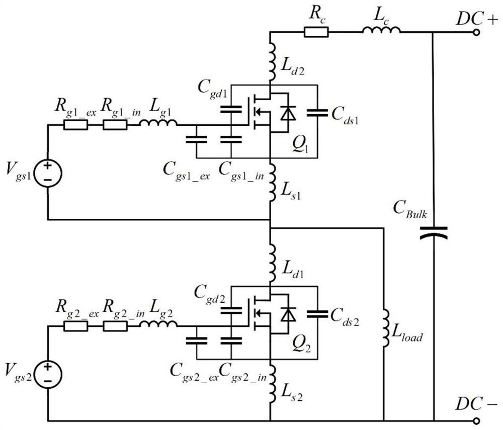
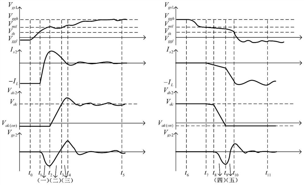
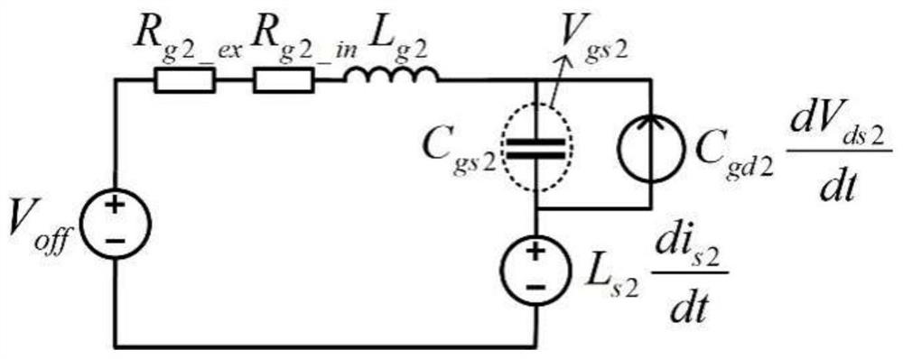
[0053] like figure 1 As shown, the double-pulse test circuit is a common circuit to verify the driving performance and obtain the dynamic characteristics of SiC MOSFET. The subscript ex means the outside of the power tube; the subscript in means the inside of the power tube, and all internal device parameters cannot be adjusted.

[0054] Build a half-bridge double-pulse test circuit, which inc...


PUM


Abstract

The invention discloses a SiC MOSFET crosstalk voltage calculation, parasitic parameter extraction and driving parameter setting method, and belongs to the technical field of wide bandgap semiconductor device driving. According to the technical scheme, the SiC MOSFET crosstalk voltage model considering the common-source inductance is simplified, a SiC MOSFET crosstalk voltage model is combined with an actual crosstalk voltage suppression method, a driving loop lumped parameter combination with the best crosstalk voltage suppression effect is found through an optimization solution method, timeand devices consumed by repeatedly replacing elements for double-pulse testing in the hardware debugging stage are greatly reduced, the hardware design efficiency is improved, and the parameter setting process is simplified.

Description

technical field [0001] The invention belongs to the technical field of driving wide bandgap semiconductor devices, and more specifically relates to methods for calculating SiC MOSFET crosstalk voltage, extracting parasitic parameters and setting driving parameters. Background technique [0002] SiC MOSFET is a representative device of the third-generation wide bandgap semiconductor, which is widely used because of its high-speed switching capability, low conduction loss, high junction temperature, and high withstand voltage. However, due to the high-speed switching of SiC MOSFET as an action device, the parasitic parameters introduced by device packaging and design restrictions flow through high-frequency signals, which will introduce a large impedance in the circuit and have a significant impact on device characteristics. In the bridge arm circuit, the action device will introduce a crosstalk voltage on the gate source of the off device, and the positive peak value of the c...

Claims


Application Information

Patent Timeline
Patent Type & Authority Applications(China)
IPC IPC(8): H02M1/088G01R31/28
CPCG01R31/282H02M1/088Y02B70/10
Inventor 刘恒阳孔武斌曲荣海涂钧耀
Owner HUAZHONG UNIV OF SCI & TECH
Why Eureka
Try Eureka