Multi-chip package structure having chip interconnection bridge which provides power connections between chip and package substrate

A packaging substrate and packaging structure technology, applied in the direction of circuits, electrical components, electric solid devices, etc., can solve the problems of increasing the voltage drop of the packaging substrate and IR heating

Pending Publication Date: 2021-03-16
IBM CORP
View PDF0 Cites 3 Cited by
  • Summary
  • Abstract
  • Description
  • Claims
  • Application Information

AI Technical Summary

Problems solved by technology

This configuration increases the length of the power / ground traces and therefore increases the voltage drop and IR heating within the package substrate

Method used


Image

  • Multi-chip package structure having chip interconnection bridge which provides power connections between chip and package substrate
  • Multi-chip package structure having chip interconnection bridge which provides power connections between chip and package substrate
  • Multi-chip package structure having chip interconnection bridge which provides power connections between chip and package substrate

Examples


Embodiment Construction

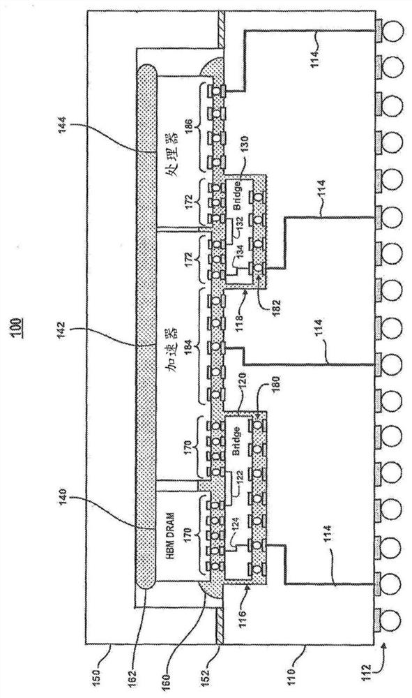
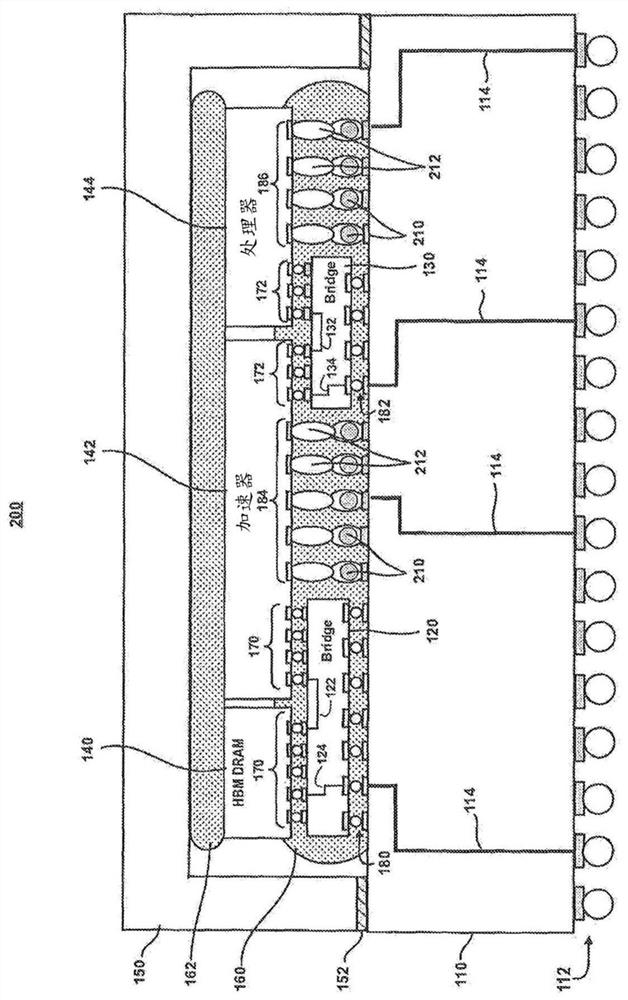
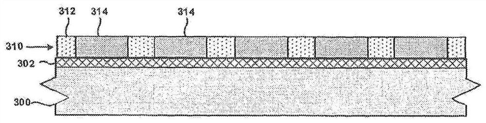
[0027] An embodiment of the present invention will now be discussed in more detail with respect to the multi-chip package structure, which includes a chip interconnect device, which is designed to be used between adjacent chips in the package structure. High I / O interconnect density is provided, and a vertical power distribution trace is provided by the chip's interconnect device to supply a power source (and ground) from the package substrate to the chip to the chip interconnect device. It should be understood that the individual layers, structures, and regions shown in the drawings are illustrative diagrams that are not drawn. Furthermore, in order to facilitate explanation, one or more layers, structures, and regions that are typically used to form a type of semiconductor device or structure may not be explicitly shown in the given drawings. This does not mean any layers, structures, and regions that are not explicitly shown from the actual semiconductor structure.

[0028]Fu...


PUM


Abstract

Multi-chip package structures and methods for constructing multi-chip package structures are provided, which utilize chip interconnection bridge devices that are designed to provide high interconnectdensity between adjacent chips (or dies) in the package structure, as well as provide vertical power distribution traces through the chip interconnection bridge device to supply power (and ground) connections from a package substrate to the chips connected to the chip interconnection bridge device.

Description

Technical field [0001] The present disclosure involves semiconductor package techniques, and specifically, the multi-chip package structure of a chip interconnect device is referred to. Background technique [0002] Innovation in Semiconductor Manufacturing and Packaging Technology has enabled minimal size, higher density integrated circuit (IC) chip (or die), and development has wiring and area that enables intensive encapsulation IC chip (or die). A high integrated chip module of the array input / output (I / O) contact density. For some applications, a suitable area array connection technique for module to board I / O interconnection (eg, pad grid array (LGA) or ball grid (BGA) is used, with a circuit board (for example, , One or more multi-chip modules (MCM) of the system board (or node card), printed circuit board, printed wiring board, etc.) to construct high performance electronic modules. The MCM technology can be used to form a first level package structure having a plur...

Claims


Application Information

Patent Timeline
Patent Type & Authority Applications(China)
IPC IPC(8): H01L23/538H01L25/065
CPCH01L23/055H01L23/04H01L21/6835H01L2221/68381H01L2221/68345H01L23/3737H01L23/3675H01L23/5385H01L23/49816H01L23/5383H01L21/4857H01L2224/16227H01L2924/15311H01L2224/1132H01L2224/11332H01L2224/133H01L2224/13294H01L2224/11462H01L2224/13082H01L2224/32225H01L2224/73204H01L2224/32245H01L2224/2929H01L2224/29299H01L2224/73253H01L2224/33181H01L2224/29076H01L2224/33505H01L2224/32013H01L2224/32105H01L2224/32106H01L2224/32058H01L2224/81193H01L2224/13147H01L2224/136H01L24/13H01L24/16H01L2224/1703H01L2224/17051H01L2224/81815H01L2224/81203H01L24/81H01L24/29H01L24/32H01L24/73H01L2224/1146H01L2224/13155H01L2224/13144H01L2224/13111H01L24/14H01L2224/1403H01L2224/81005H01L24/11H01L24/17H01L2924/15192H01L2924/381H01L2224/131H01L2924/00014H01L2924/014H01L2224/16225H01L2924/00H01L23/5381H01L21/50H01L23/12
Inventor J.鲁宾L.克莱文格C.L.阿尔文
Owner IBM CORP
Why Eureka
Try Eureka