Method and device for etching silicon oxide
A technology of silicon oxide and silicon oxide film, applied in chemical instruments and methods, surface etching compositions, electrical components, etc., can solve problems such as wafer electrical damage and adverse effects of chemical solutions
- Summary
- Abstract
- Description
- Claims
- Application Information
AI Technical Summary
Problems solved by technology
Method used
Image
Examples
no. 1 Embodiment approach
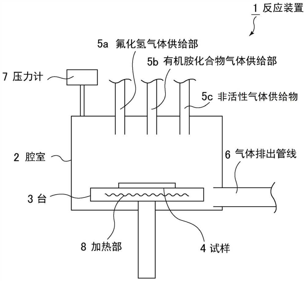
[0032] In the first embodiment, the silicon oxide is etched by supplying a processing gas (dry etching gas) containing hydrogen fluoride and an organic amine compound to the etching device and bringing it into contact with the silicon oxide.
[0033] When the silicon oxide is brought into contact with a processing gas containing hydrogen fluoride and an organic amine compound, the silicon oxide, hydrogen fluoride and the organic amine compound undergo a chemical reaction to become a reaction product such as an organic amine salt of hexafluorosilicic acid. The silicon oxide is removed by sublimation to gas or thermal decomposition to gas while generating the reaction product. It should be noted that, in the present disclosure, sublimation refers not only to the case where a solid is not thermally decomposed but becomes a gas, but also sometimes includes a case where a solid is thermally decomposed and becomes a gas component.
[0034] As the processing gas, hydrogen fluoride ga...
no. 2 Embodiment approach
[0054] A second embodiment of the dry etching method of the present disclosure is a method of separately supplying a processing gas containing an organic amine compound and a processing gas containing hydrogen fluoride to an etching device to perform etching. That is, in the second embodiment, after the step of supplying the processing gas containing the organic amine compound in the silicon oxide to the etching device, the step of supplying the processing gas containing hydrogen fluoride to the etching device is performed. A vacuuming step may be performed between the above two steps.
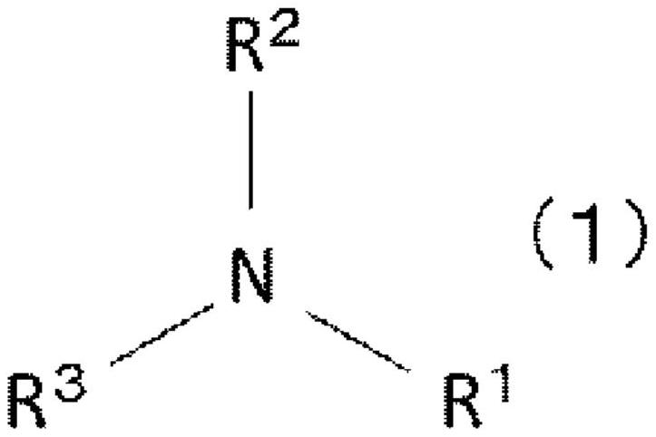
[0055] As the above-mentioned organic amine compound, a compound represented by the general formula (1) shown in the first embodiment can be used.
[0056] It is considered that the organic amine compound is adsorbed on the surface of the silicon oxide when the organic amine is initially introduced into the etching apparatus and the silicon oxide is brought into contact with the gaseous organi...
Embodiment 1-1~1-11、 comparative example 1-1~1-8
[0078] First, wafers A to C were placed on the stage in the chamber, and after the chamber was evacuated, the temperature of the stage was set to a predetermined temperature shown in Table 1 below. After that, process gas was supplied into the chamber and maintained for 30 seconds. Thereafter, after the chamber was evacuated to 10 Pa or less and replaced with an inert gas, wafers A to C were taken out, and respective film thicknesses were measured to evaluate the amount of etching. In addition, the surface of the silicon wafer B on which the thermally oxidized film was etched was observed with an optical microscope to evaluate the presence or absence of residues on the surface.
[0079] The type of organic amine, the flow rate, the flow rate of HF, the pressure during etching, the temperature, the etching time, and the evaluation results after etching are shown in Table 1 below.
[0080] In Example 1-1, HF gas and trimethylamine gas were simultaneously supplied to the chamber...
PUM
 Abstract
Description
Claims
Application Information


